PCB is the abbreviation of Printed Circuit Board. Also known as printed circuit board or printed circuit board. it is called a “printed” circuit board because it is made using electronic printing. A printed circuit board is a substrate used for assembling electronic components.
1. Printed circuit board (PCB)
It is a printed board that forms point connections and printed components on a universal base material according to a predetermined design. The main function of this product is to connect various electronic components to form a predetermined circuit and play the role of relay transmission.
It is a key electronic interconnection component of electronic products and is known as the “mother of electronic products”. PCB serves as the substrate and key interconnect for electronic components, and is required for any electronic equipment or product.
2. PCB manufacturing principles
When we open the keyboard of a general-purpose computer, we can see a soft film (flexible insulating substrate) printed with silver-white (silver paste) conductive patterns and key patterns. Because this pattern is obtained by the common screen printing method, we call this printed circuit board a flexible silver paste printed circuit board.
The various computer motherboards, graphics cards, network cards, modems, sound cards and printed circuit boards on household appliances we see in computer stores are different.
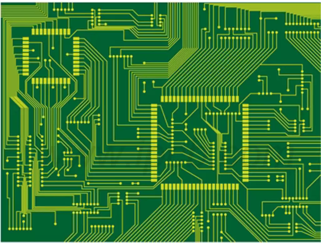
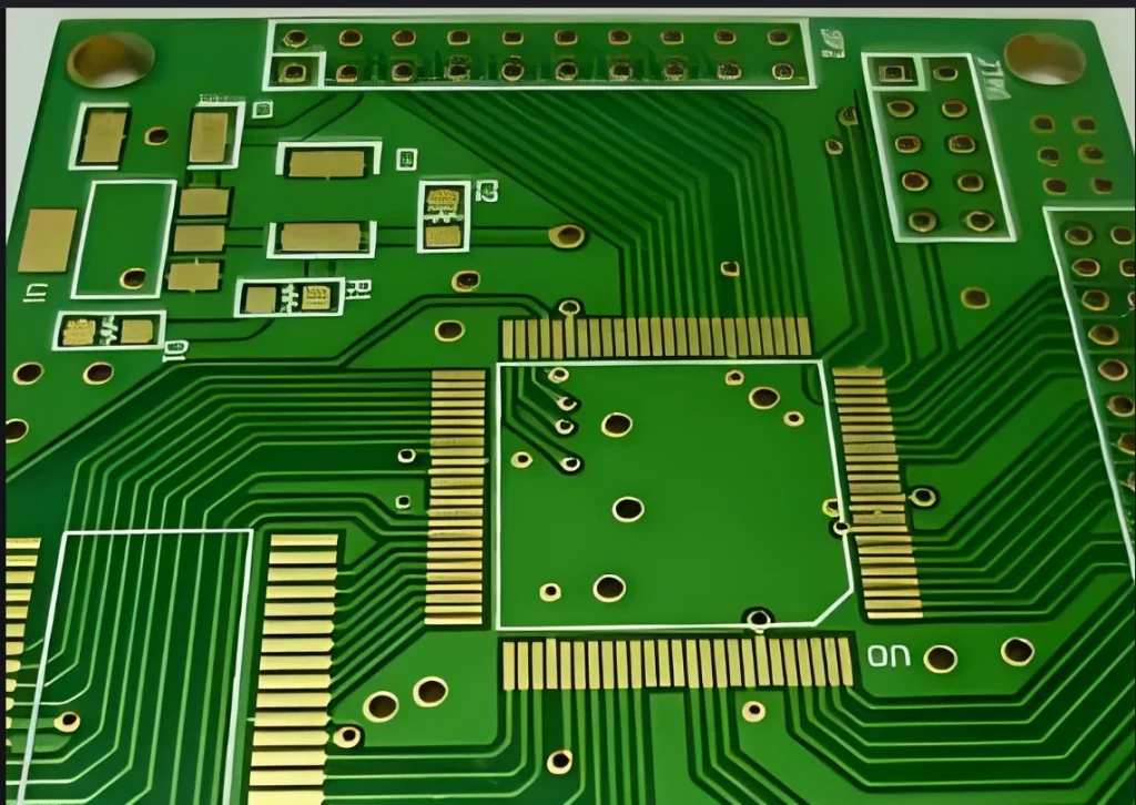
The base material used is paper base (commonly used for single-sided) or glass cloth base (commonly used for double-sided and multi-layer), pre-impregnated with phenolic or epoxy resin, and one or both sides of the surface are adhered to a copper-clad film and then laminated and cured. Become.
This kind of circuit board copper-clad sheet is called a rigid board. When it is made into a printed circuit board, we call it a rigid printed circuit board. A printed circuit board with a printed circuit pattern on one side is called a single-sided printed circuit board, and a printed circuit board with printed circuit patterns on both sides and double-sided interconnection through metallization of holes is called a double-sided board.
If one double-sided printed circuit board is used as the inner layer and two single-sided printed circuit boards are used as the outer layer, or two double-sided printed circuit boards are used as the inner layer and two single-sided printed circuit boards are used as the outer layer,
the positioning system and the insulating adhesive material are alternated together and Printed circuit boards in which conductive patterns are interconnected according to design requirements become four-layer or six-layer printed circuit boards, also known as multi-layer printed circuit boards. There are now more than 100 layers of practical printed circuits.
3. Characteristics and classification of PCB
PCB features include high density, high reliability, designability, producibility, assembly and maintainability.
Generally speaking, the more complex the functions of an electronic product, the longer the loop distance, and the greater the number of contact pins, the more layers of PCB are required, such as high-end consumer electronics, information and communication products, etc.;
And soft boards are mainly used for needs Among the products that are used for bending; such as notebook computers, cameras, automobile instruments, etc. PCB is classified according to the number of layers and can be divided into single-sided boards (SSB), double-sided boards (DSB) and multi-layer boards (MLB); according to softness,
it can be divided into rigid printed circuit boards (RPC) and flexible printed circuits. Board (FPC). In industrial research, generally according to the basic classification of PCB products mentioned above, the PCB industry is subdivided into six main subdivisions: single-sided panels, double-sided boards, conventional multi-layer boards, flexible boards, HDI (high-density sintering) boards, and packaging substrates.
The PCB upstream industry includes PCB base material board raw material suppliers and PCB production equipment suppliers, and the downstream industries include consumer electronics, computers and peripheral products, automobile industry and mobile phone industry.
According to the industrial chain, it can be divided into raw materials – copper clad laminates – printed circuit boards – electronic product applications. The specific analysis is as follows:
Fiberglass cloth: Fiberglass cloth is one of the raw materials of copper-clad laminates. It is woven from fiberglass yarn and accounts for about 40% (thick plate) and 25% (thin plate) of the cost of copper-clad laminate.
Fiberglass yarn is calcined into a liquid state in a kiln from silica sand and other raw materials, and then drawn into extremely fine glass fibers through a very small alloy nozzle, and then hundreds of glass fibers are twisted into fiberglass yarn.
Copper foil: Copper foil is the raw material that accounts for the largest proportion of the cost of copper clad laminates, accounting for approximately 30% (thick plate) and 50% (thin plate) of the cost of copper clad laminates. Therefore, the price increase of copper foil is the main driving force for the price increase of copper clad laminates.
Copper-clad laminate: Copper-clad laminate is a product made of fiberglass cloth and copper foil pressed together using epoxy resin as a fusion agent. It is the direct raw material of PCB. It is made into a printed circuit after etching, electroplating, and lamination of multi-layer boards.
The above is my understanding and sharing of printed circuit board circuits, thank you.