Complete Interpretation of ROHS PCB Design and Manufacturing
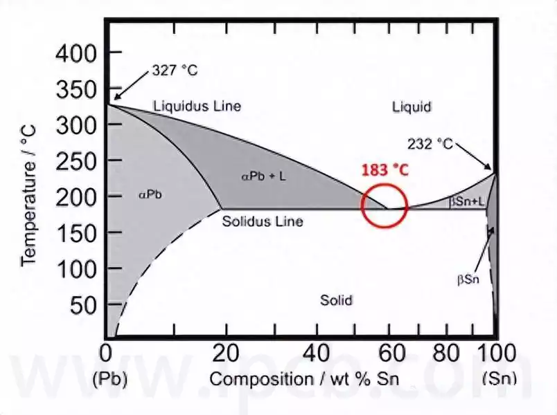
Introduction With the continuous improvement of global environmental awareness, green manufacturing has become an irreversible trend in the electronics industry. Major markets such as Europe and the United States have put forward stricter environmental standards for electronic products. Among them, ROHS PCB, as a basic compliance requirement, is playing the dual role of “pass” and […]