Historical Evolution
The story of electronic print boards, commonly known as printed circuit boards (PCBs), begins in the early 20th century. Initially, electronics were assembled using point-to-point wiring, a labor-intensive and error-prone method. The first conceptual step towards electronic print boards was taken by Albert Hanson, a German inventor, in 1903. Hanson described flat foil conductors laminated to an insulating board in multiple layers, a rudimentary idea that would later evolve into the multi-layer PCBs we use today.
During the 1920s and 1930s, further developments were made, including the creation of the substrate materials and the introduction of etched traces. However, it was Paul Eisler, an Austrian engineer, who is credited with the invention of the modern electronic print board. In 1943, while working on a radio set for the British military, Eisler developed a method of printing conductive tracks on a non-conductive base material. This innovation significantly reduced the complexity and cost of electronic assemblies.
Post-World War II, the use of electronic print boards expanded rapidly. The US military recognized their potential and adopted them for various applications. The 1950s and 1960s saw the commercialization of PCBs, with industries such as telecommunications and consumer electronics integrating them into their products. The advent of integrated circuits (ICs) further propelled the demand for sophisticated PCB designs.
The journey of electronic print boards from a conceptual idea to a cornerstone of modern electronics is a testament to human ingenuity and technological progress. As we continue to innovate and push the boundaries of what is possible, the role of PCBs in our technological ecosystem remains as vital as ever.
Design Principles
The design of an electronic print board is a meticulous process that involves several key steps and principles. A well-designed PCB ensures the reliable operation of the electronic device, minimizes electromagnetic interference (EMI), and optimizes the performance of the circuit.
Schematic Capture
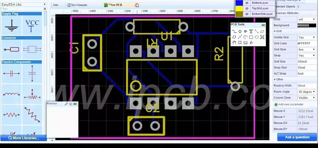
The design process begins with schematic capture, where engineers create a detailed diagram of the circuit. This schematic includes all the electronic components, such as resistors, capacitors, ICs, and their connections. Schematic capture software helps designers visualize the circuit and make necessary adjustments before moving to the layout stage.
Component Placement
Once the schematic is finalized, the next step is component placement. This involves strategically positioning the components on the electronic print board to ensure efficient routing of connections, thermal management, and mechanical stability. Proper component placement is crucial for minimizing noise, crosstalk, and other electrical issues.
Routing
Routing is the process of connecting the components with copper traces on the electronic print board. This step requires careful planning to avoid signal integrity problems. Designers use various routing strategies, such as single-layer, double-layer, or multi-layer routing, depending on the complexity of the circuit. High-speed circuits may require controlled impedance routing to ensure signal quality.
Design Rule Checks
Before finalizing the design, engineers perform design rule checks (DRCs) to ensure that the electronic print board meets all the manufacturing and electrical requirements. DRCs verify aspects such as trace width, spacing, hole size, and component clearances. Any violations must be corrected to avoid manufacturing defects and operational failures.
Gerber Files
The final step in the design process is the creation of Gerber files. These files contain the detailed information required by PCB manufacturers to fabricate the board. Gerber files include data on copper layers, solder masks, silkscreen, drill files, and other essential details. Accurate Gerber files are critical for ensuring that the electronic print board is manufactured as intended.
Manufacturing Processes
The journey from an electronic print board design to a tangible product involves several intricate manufacturing processes. Each step must be executed with precision to ensure the quality and reliability of the final PCB.
Substrate Preparation
The manufacturing process begins with substrate preparation. The substrate, typically made of fiberglass-reinforced epoxy resin (FR-4), serves as the base material for the electronic print board. The substrate is cut into panels of the desired size, and its surface is cleaned to remove any contaminants.
Copper Lamination
Next, a thin layer of copper is laminated onto the substrate. This copper layer will form the conductive traces of the electronic print board. The lamination process involves applying heat and pressure to bond the copper to the substrate securely. Multi-layer PCBs require additional layers of copper and insulating material to be laminated together.
Image Transfer
The image transfer process involves transferring the PCB design onto the copper-clad substrate. This is typically done using a photolithographic technique. A photoresist material is applied to the copper surface, and the PCB design is projected onto the substrate using ultraviolet (UV) light. The exposed photoresist hardens, while the unexposed areas remain soft and are subsequently washed away, leaving behind the pattern of the copper traces.
Etching
Etching is the process of removing unwanted copper from the substrate, leaving only the desired traces. The board is immersed in an etching solution, typically a ferric chloride or ammonium persulfate solution, which dissolves the unprotected copper. The etched board is then cleaned to remove any residual chemicals.
Drilling
After etching, the next step is drilling. Holes are drilled into the PCB to accommodate through-hole components and vias, which provide electrical connections between different layers of the electronic print board. High-precision CNC machines are used to drill these holes accurately.
Plating
The drilled holes are then plated with copper to establish electrical connections. The entire PCB is submerged in an electroplating bath, where a thin layer of copper is deposited onto the exposed surfaces, including the hole walls. This process ensures reliable electrical continuity between the layers of the electronic print board.
Solder Mask Application
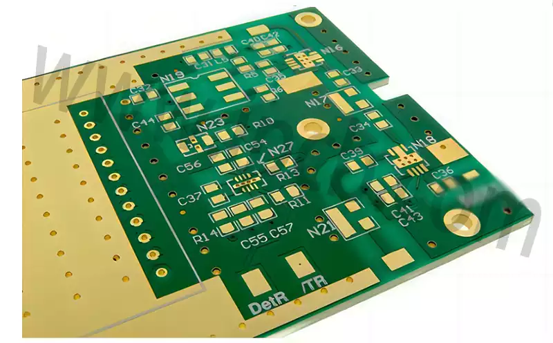
A solder mask is applied to the PCB to protect the copper traces from oxidation and prevent solder bridges during component assembly. The solder mask is typically a green (though other colors are available) epoxy-based layer that covers the entire board except for the pads and vias. The solder mask is applied using a screen-printing process and then cured using UV light or heat.
Silkscreen Printing
Silkscreen printing is used to apply text and symbols on the PCB, providing important information such as component labels, part numbers, and logos. This step is crucial for the assembly and debugging processes. The silkscreen is applied using a screen-printing process, similar to the solder mask application.
Surface Finish
To ensure good solderability and protect the exposed copper, a surface finish is applied to the PCB. Common surface finishes include Hot Air Solder Leveling (HASL), Electroless Nickel Immersion Gold (ENIG), and Organic Solderability Preservative (OSP). Each finish has its advantages and is chosen based on the specific requirements of the application.
Testing
The final step in the manufacturing process is testing. Various tests are conducted to verify the electrical integrity and functionality of the PCB. Common tests include electrical testing, in-circuit testing (ICT), and functional testing. These tests help identify any manufacturing defects or issues that could affect the performance of the electronic print board.
Diverse Types
PCBs come in a myriad of forms, each tailored to meet the unique demands of its application. From the simplicity of single-sided boards to the complexity of multi-layer marvels, electronic print boards offer a canvas for creativity and innovation. With advancements in technology, new frontiers in PCB design continue to emerge, pushing the boundaries of what is possible.
Single-Sided PCBs are the most basic type, featuring a single layer of conductive copper on one side of the substrate. They are used in simple, low-cost electronics such as calculators, power supplies, and household appliances. Their straightforward design makes them easy to manufacture and cost-effective.
Double-Sided PCBs have copper layers on both sides of the substrate, allowing for more complex circuitry and increased component density. Vias, small plated holes, are used to create electrical connections between the two layers. Double-sided PCBs are commonly used in applications such as power monitoring, test equipment, and automotive electronics.
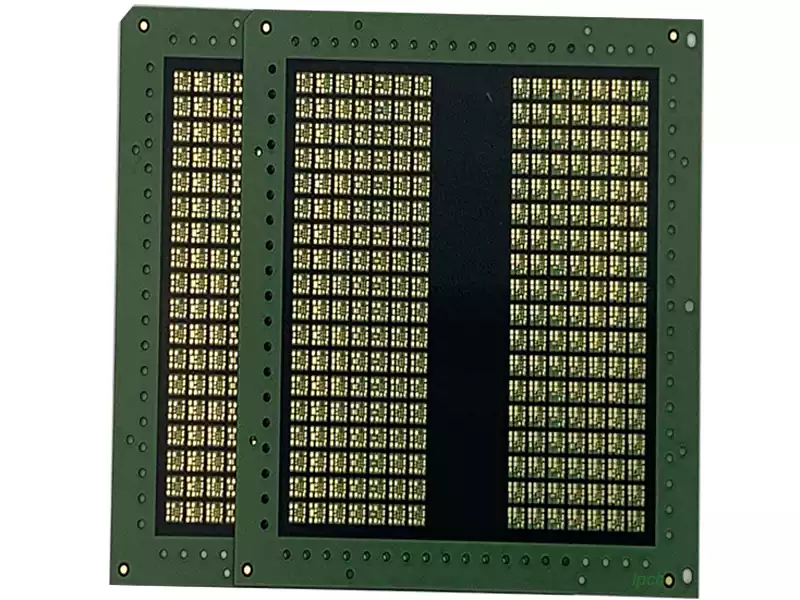
Multi-layer PCBs consist of multiple layers of copper and insulating material stacked together. These PCBs can have anywhere from three to over fifty layers, enabling the integration of highly complex circuits. Multi-layer PCBs are essential in advanced electronics, including computer motherboards, medical devices, and communication equipment.
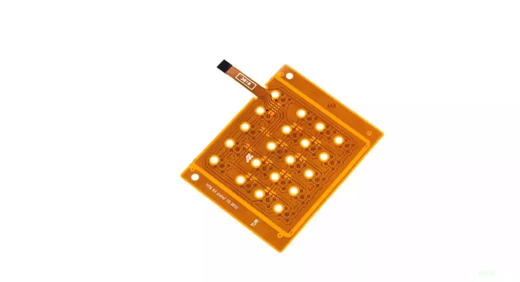
Flexible PCBs, or flex PCBs, are made of flexible plastic substrates, such as polyimide, allowing them to bend and flex. They are used in applications where space and flexibility are critical, such as wearable devices, foldable smartphones, and aerospace electronics. Flex PCBs can be single-sided, double-sided, or multi-layered.
Rigid-flex PCBs combine the advantages of rigid and flexible PCBs, incorporating both rigid and flexible sections in a single board. This hybrid design provides the flexibility needed for complex assemblies while maintaining the rigidity required for component support. Rigid-flex PCBs are used in advanced applications like military systems, medical devices, and portable electronics.
HDI PCBs are characterized by their high component density and fine trace widths. They utilize advanced manufacturing techniques such as laser drilling and microvias to achieve high interconnect density. HDI PCBs are used in cutting-edge electronics like smartphones, tablets, and other high-performance devices.
Ubiquitous Applications
The ubiquity of electronic print boards is a testament to their versatility and utility. From the smartphones that connect us to the world to the advanced machinery that drives our industries, electronic print boards are the silent heroes of modern technology. Their presence is felt across a multitude of sectors, each benefiting from their reliability and efficiency.
In consumer electronics, electronic print boards are found in smartphones, tablets, laptops, and televisions, where they serve as the backbone of the device, providing connectivity and functionality. In the automotive industry, PCBs are used in engine control units (ECUs), infotainment systems, and advanced driver assistance systems (ADAS), enhancing safety and performance.
In the aerospace and defense sectors, electronic print boards are used in avionics, radar systems, and missile guidance systems, where reliability and durability are paramount. In the medical field, PCBs are found in diagnostic equipment, patient monitoring devices, and medical imaging systems, helping healthcare professionals provide accurate diagnoses and treatments.
Furthermore, electronic print boards play a crucial role in industrial automation, robotics, and IoT (Internet of Things) applications, where they enable seamless communication and control of complex systems. From smart home devices to industrial machinery, PCBs enable the automation and optimization of processes, increasing efficiency and productivity.
As technology continues to advance, the demand for electronic print boards will only continue to grow. From the smallest wearable devices to the largest industrial machines, electronic print boards will remain at the heart of innovation, driving progress and shaping the future of technology.
Conclusion
In conclusion, electronic print boards have evolved from simple prototypes to essential components found in a wide array of electronic devices, driving innovation across industries. As technology advances, PCBs will continue to play a vital role in shaping the future of electronics, enabling the development of more sophisticated and powerful systems that improve efficiency, connectivity, and functionality.