In the realm of Printed Circuit Board (PCB) design and manufacturing, minimum solder mask sliver is a critical parameter that directly influences the reliability and performance of electronic devices. This term refers to the smallest permissible gap between solder mask layers covering conductive features like pads, traces, and vias on a PCB. Managing minimum solder mask sliver effectively is essential to prevent solder bridging during assembly and to ensure the overall quality of the PCB.
Introduction to Solder Mask and Its Importance
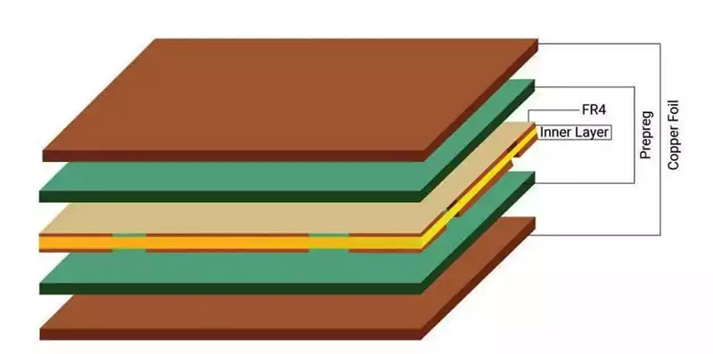
The solder mask is a protective layer applied over the copper traces and pads on a PCB. It serves several crucial functions:
- Preventing Solder Bridges: During soldering, the solder mask prevents solder from flowing between closely spaced conductive features, thereby preventing unintended electrical connections or short circuits.
- Insulating and Protecting: It provides insulation between conductive features, preventing electrical shorts and ensuring the PCB operates reliably under various conditions.
- Enhancing Alignment and Solderability: The solder mask aids in accurately aligning solder during assembly and improves the solderability of exposed copper areas.
Importance of Minimum Solder Mask Sliver
The effectiveness of the solder mask in fulfilling its protective and insulating functions hinges on minimum solder mask sliver. This parameter dictates the smallest allowable gap between adjacent solder mask openings or between solder mask and copper features. It is crucial to adhere to specified minimum solder mask sliver requirements to:
- Ensure Manufacturing Consistency: Adequate gap size facilitates uniform and complete coverage of the solder mask during processes such as screen printing or spray coating.
- Mitigate Electrical Issues: Inadequate minimum solder mask sliver can lead to mask fractures or insufficient coverage, potentially causing electrical shorts or reliability issues in the PCB.
Factors Influencing Minimum Solder Mask Sliver
Several factors influence the determination of minimum solder mask sliver:
- PCB Design Considerations: The layout and spacing of pads, traces, and vias play a crucial role in defining minimum solder mask sliver requirements. Designers must consider these factors based on the capabilities of the chosen solder mask material and manufacturing process.
- Manufacturing Capabilities: Different PCB manufacturers may have varying capabilities in achieving the minimum solder mask sliver. Collaboration with manufacturers ensures alignment with their production capabilities and quality standards.
- Material Properties: The type and quality of solder mask material significantly impact minimum solder mask sliver. High-quality materials with good adhesion properties and resistance to cracking under thermal stress are essential for long-term reliability.
Design Guidelines for Managing Minimum Solder Mask Sliver
To optimize minimum solder mask sliver, designers should consider the following guidelines:
- Follow Manufacturer Specifications: Consult PCB manufacturer specifications for recommended minimum solder mask sliver values based on the chosen solder mask material and manufacturing process.
- Avoid Narrow Gaps: Design layouts that minimize narrow gaps between solder mask openings and adjacent conductive features to reduce the risk of insufficient coverage or mask fractures.
- Implement Design Rule Checks (DRC): Use design rule checks to verify compliance with minimum solder mask sliver requirements throughout the PCB layout process.
- Prototype and Test: Prototype PCBs should undergo rigorous testing to validate solder mask integrity, including its ability to withstand thermal cycling and mechanical stress without developing cracks or defects.
Challenges in Managing Minimum Solder Mask Sliver
Managing minimum solder mask sliver effectively can be challenging due to several factors:
- Complex PCB Designs: As PCBs become more complex with higher component densities and finer traces, maintaining adequate solder mask sliver becomes more difficult. Designers need to carefully balance the need for compact layouts with the requirements for sufficient solder mask coverage.
- Variability in Manufacturing Processes: Different manufacturing processes and equipment can lead to variability in the application of solder mask. This variability can affect the consistency of the solder mask sliver and requires stringent quality control measures.
- Environmental Factors: Environmental factors such as temperature and humidity can impact the performance and reliability of the solder mask. Ensuring that the solder mask can withstand these conditions without degrading is essential for maintaining adequate sliver.
Case Studies and Real-World Applications
In practical scenarios, adherence to appropriate minimum solder mask sliver values has been instrumental in enhancing PCB reliability and performance. For example, in high-frequency and high-speed PCBs used in telecommunications and data communication systems, maintaining precise solder mask sliver is crucial to prevent signal interference and ensure signal integrity.
Another case involves automotive electronics, where PCBs are subjected to harsh environments with high temperatures and vibrations. Ensuring adequate solder mask sliver helps protect the PCB from environmental stress, enhancing the reliability and longevity of automotive electronic systems.
Advances in Solder Mask Technologies
Recent advances in solder mask technologies have also contributed to better management of minimum solder mask sliver. Innovations such as laser direct imaging (LDI) and advanced photopolymer solder masks allow for more precise application and control of solder mask layers. These technologies enable finer resolution and better adherence to design specifications, reducing the risk of solder mask defects and improving overall PCB quality.
Future Trends and Considerations
Looking forward, the trend towards miniaturization and increased functionality in electronic devices will continue to push the boundaries of PCB design and manufacturing. As components become smaller and more densely packed, maintaining adequate minimum solder mask sliver will remain a critical challenge. Ongoing research and development in solder mask materials and application techniques will be essential to meet these demands.
Conclusion
In conclusion, minimum solder mask sliver is a crucial aspect of PCB design and manufacturing that directly impacts the reliability and performance of electronic devices. Designers must carefully manage this parameter to ensure adequate protection, prevent electrical issues, and enhance overall PCB reliability. By adhering to recommended guidelines and collaborating closely with PCB manufacturers, designers can optimize PCB layouts for optimal minimum solder mask sliver performance, contributing to advancements in electronic device technology.