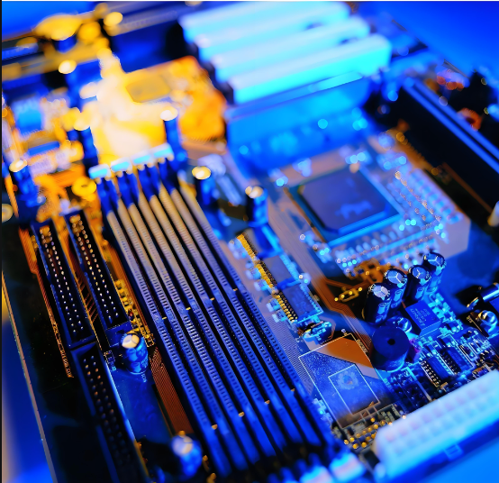
In the fast-evolving world of electronics, printed circuit boards (PCBs) form the backbone of virtually all electronic devices. From simple gadgets like digital clocks to complex systems like smartphones and computers, PCBs are essential.
PCB board makers, the specialized companies and engineers responsible for designing and manufacturing these critical components, play a pivotal role in the electronics industry. This article delves into the world of PCB board makers, exploring their processes, challenges, and the innovations driving the industry forward.
Understanding PCBs: The Heart of Electronic Devices
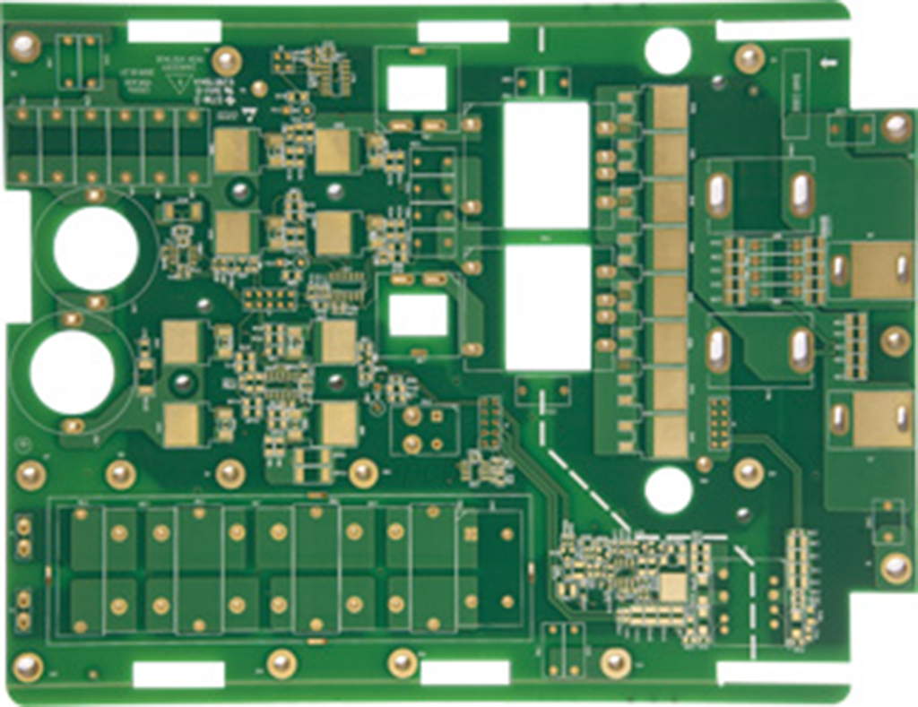
A PCB is a flat board used to physically support and electrically connect electronic components. They are composed of an insulating substrate, typically fiberglass, and have conductive pathways etched from copper sheets laminated onto a non-conductive substrate. Components such as resistors, capacitors, and integrated circuits (ICs) are soldered onto the PCB, creating a complete circuit.
PCBs can be single-sided, double-sided, or multilayered, depending on the complexity and the requirements of the electronic device they are intended for. Single-sided PCBs have components and copper traces on one side of the substrate, whereas double-sided PCBs have them on both sides. Multilayered PCBs, which are essential for complex devices, consist of multiple layers of substrates and circuits stacked and bonded together.
The PCB Manufacturing Process
The creation of a PCB involves several meticulous steps, each critical to the performance and reliability of the final product. Here’s a detailed look at the PCB manufacturing process:
- Design and Layout:
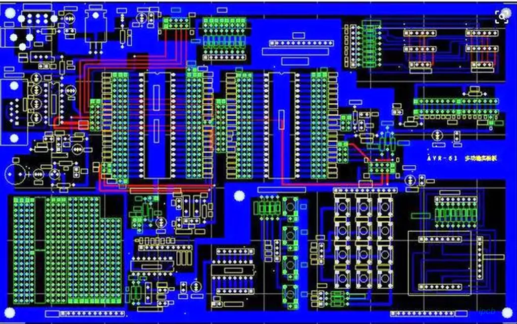
- Schematic Design: The process begins with a schematic design, which is a blueprint of the circuit showing the components and their connections. Engineers use CAD (Computer-Aided Design) software to create these schematics.
- PCB Layout: Once the schematic is complete, the next step is to create the PCB layout. This involves placing the components on the board and routing the electrical connections between them. The layout must consider factors like signal integrity, thermal management, and manufacturability.
- Material Preparation:
- Substrate Selection: The substrate, typically FR4 (a fiberglass-reinforced epoxy laminate), is chosen based on the application’s requirements. For high-frequency applications, materials with better electrical properties, like Rogers or Teflon, may be used.
- Copper Cladding: The selected substrate is coated with a thin layer of copper on one or both sides.
- Image Transfer:
- Photoresist Application: A photoresist, a light-sensitive material, is applied to the copper-clad substrate.
- Exposure and Development: The photoresist-coated substrate is then exposed to ultraviolet (UV) light through a photomask that contains the circuit pattern. The exposed areas of the photoresist harden, and the unexposed areas are washed away, leaving the copper exposed in the pattern of the circuit.
- Etching:
- The exposed copper is etched away using a chemical solution, leaving behind the desired copper traces. The remaining photoresist is then removed.
- Drilling:
- Precision drilling machines create holes for component leads and vias (connections between different layers in multilayer PCBs). The accuracy and quality of drilling are crucial for the board’s functionality.
- Plating and Coating:
- The drilled holes are plated with copper to create electrical connections between layers. Additional plating, like tin-lead or gold, may be applied for better solderability and corrosion resistance.
- A solder mask, a protective coating, is applied to prevent short circuits and protect the copper traces.
- Silkscreen Printing:
- Important information, such as component identifiers and company logos, is printed onto the board using a silkscreen process.
- Testing:
- The finished PCBs undergo rigorous testing to ensure they meet design specifications and are free from defects. Electrical tests, such as flying probe tests or in-circuit tests, verify the connectivity and performance of the circuits.
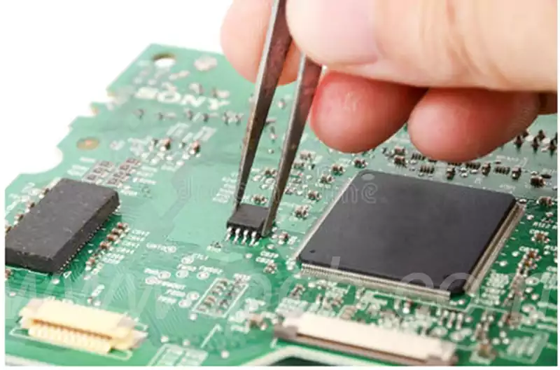
- Assembly:
- Components are placed onto the PCB and soldered in place. This can be done through manual soldering for small-scale production or automated processes like Surface Mount Technology (SMT) for larger volumes.
Challenges Faced by PCB Board Makers
PCB manufacturing is a complex and demanding process, and PCB board makers face numerous challenges, including:
- Miniaturization: With the trend towards smaller and more powerful devices, PCB makers must create boards with finer traces and smaller components, increasing the risk of manufacturing defects and requiring more precise equipment and techniques.
- High-Density Interconnects (HDI): As devices become more sophisticated, the need for HDI PCBs, which have a higher density of wiring per unit area, increases. This requires advanced manufacturing capabilities and more stringent quality control.
- Thermal Management: Efficient thermal management is crucial, especially in high-power applications. PCB makers must design boards that dissipate heat effectively to prevent component failure.
- Material Selection: Choosing the right materials for specific applications is critical. The materials must meet the electrical, thermal, and mechanical requirements of the device while remaining cost-effective.
- Environmental Regulations: PCB manufacturers must comply with strict environmental regulations regarding the use of hazardous materials and waste disposal. This adds complexity and cost to the manufacturing process.
- Supply Chain Management: Ensuring a steady supply of high-quality materials and components is essential. Disruptions in the supply chain can lead to delays and increased costs.
Innovations and Future Trends in PCB Manufacturing
The PCB manufacturing industry is continually evolving, driven by technological advancements and the ever-increasing demand for more powerful and compact electronic devices. Some key innovations and trends shaping the future of PCB manufacturing include:
- Flexible PCBs: Flexible PCBs, which can be bent and folded, are gaining popularity in applications like wearable devices and flexible displays. They offer significant advantages in terms of space savings and mechanical durability.
- Rigid-Flex PCBs: Combining the best of both rigid and flexible PCBs, rigid-flex PCBs are used in applications where both flexibility and rigidity are required. They are commonly used in aerospace, medical devices, and military applications.
- Advanced Materials: The development of new materials with superior electrical and thermal properties is enabling the creation of high-performance PCBs for demanding applications like 5G communications, automotive electronics, and IoT devices.
- 3D Printing: Additive manufacturing or 3D printing is being explored for PCB production. This technology can potentially reduce manufacturing time and costs, especially for prototype and small-batch production.
- Embedded Components: Integrating passive and active components directly into the PCB substrate is an emerging trend. This approach can significantly reduce the size and weight of electronic devices while improving performance.
- Artificial Intelligence and Automation: AI and automation are transforming the PCB manufacturing process. Automated inspection systems, predictive maintenance, and AI-driven design tools are improving efficiency, reducing defects, and shortening time-to-market.
- Environmental Sustainability: PCB manufacturers are increasingly adopting eco-friendly practices, such as using lead-free solder, reducing waste, and recycling materials. Sustainability is becoming a critical factor in the industry.
Conclusion
PCB board makers are at the forefront of technological innovation, enabling the rapid advancement of electronic devices that define modern life. From meticulous design and material selection to advanced manufacturing processes and stringent quality control, the role of PCB makers is both complex and indispensable.
As the demand for smaller, faster, and more reliable electronic devices continues to grow, PCB board makers will remain essential players in the ongoing technological revolution. Their ability to innovate and adapt to new challenges will determine the future landscape of the electronics industry.