Flip chip technology, also known as controlled collapse chip connection (C4), represents a revolutionary approach in the field of electronic packaging. It involves mounting a semiconductor device or integrated circuit (IC) face down directly onto the substrate or circuit board, with the electrical connections made through solder bumps. This method has been instrumental in driving advancements in miniaturization, performance enhancement, and reliability of electronic devices.
Historical Overview and Evolution
The origins of flip chip technology date back to the 1960s when IBM first introduced the concept to overcome the limitations of traditional wire bonding methods. Initially developed for mainframe computers, the technology has since evolved significantly. Early implementations were limited by the materials and fabrication techniques available at the time. However, advancements in materials science, semiconductor fabrication, and assembly processes have dramatically improved the performance and reliability of flip chip assemblies.
Advantages of Flip Chip Technology
One of the primary advantages of flip chip technology is its ability to provide higher input/output (I/O) density compared to traditional wire bonding. By utilizing the entire surface area of the chip for connections, it allows for more interconnects in a smaller footprint, which is crucial for modern high-performance computing applications.
This increased density not only saves space but also reduces the parasitic inductance and capacitance associated with longer bond wires, leading to improved signal integrity and faster electrical performance.
Another significant benefit is the improved thermal management offered by flip chip packaging. With the active side of the die in direct contact with the substrate, heat dissipation is more efficient, enabling higher power devices to operate without overheating. This aspect is particularly important in applications such as high-performance computing, graphics processing units (GPUs), and radio-frequency (RF) components, where managing heat is critical to maintaining performance and reliability.
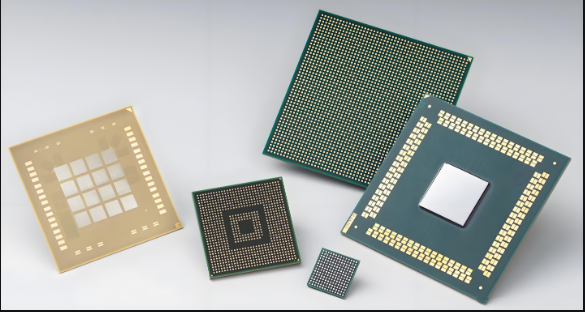
Manufacturing and Assembly Processes
The flip chip assembly process involves several key steps: wafer bumping, die preparation, flip chip attach, and reflow soldering. Wafer bumping, the first step, entails depositing solder bumps onto the die’s I/O pads. This can be achieved through various techniques, including electroplating, evaporation, and stencil printing. The choice of method depends on factors such as bump size, pitch, and material compatibility.
After bumping, the wafer is diced into individual dies, which are then flipped and aligned onto the substrate. The precise alignment of the die and substrate is crucial to ensure reliable electrical connections and mechanical stability. Following alignment, the assembly undergoes reflow soldering, where the solder bumps are melted to form metallurgical bonds with the substrate pads. This process is typically performed in a controlled atmosphere to prevent oxidation and ensure uniform solder joint formation.
Applications in Modern Electronics
Flip chip technology has found widespread adoption across various sectors of the electronics industry due to its superior performance characteristics. In consumer electronics, it is commonly used in smartphones, tablets, and wearable devices, where space constraints and performance demands are high. The technology’s ability to support high I/O counts and efficient thermal management makes it ideal for these compact, high-performance applications.
In the realm of computing, flip chip technology is a cornerstone in the development of central processing units (CPUs) and GPUs. The increased I/O density and enhanced thermal performance enable these components to handle higher processing loads and deliver faster computational speeds. Additionally, the technology is pivotal in the advancement of server and data center technologies, where performance, reliability, and power efficiency are paramount.
The automotive industry also benefits from flip chip packaging, particularly in advanced driver-assistance systems (ADAS), infotainment systems, and electric vehicle (EV) power electronics. The ruggedness and reliability of flip chip assemblies make them well-suited for the demanding environmental conditions encountered in automotive applications.
Challenges and Future Directions
Despite its numerous advantages, flip chip technology faces several challenges that need to be addressed to further its adoption. One of the primary challenges is the high initial cost associated with the fabrication and assembly processes. The precision required for wafer bumping and die alignment, as well as the need for advanced reflow soldering equipment, contribute to the overall cost. However, as the technology matures and economies of scale are realized, these costs are expected to decrease.
Another challenge is the management of mechanical stresses that arise due to the thermal expansion mismatch between the silicon die and the substrate. These stresses can lead to solder joint fatigue and eventual failure. To mitigate this, researchers are exploring the use of underfill materials, which help to distribute the stresses more evenly and enhance the mechanical robustness of the assembly.
Looking ahead, the future of flip chip technology is promising, with ongoing research and development aimed at addressing current limitations and expanding its capabilities. One area of focus is the development of new solder materials and bumping techniques to further improve reliability and performance. Additionally, advancements in substrate materials and design are expected to enhance the thermal and electrical characteristics of flip chip assemblies.
Another exciting direction is the integration of flip chip technology with emerging packaging approaches, such as 2.5D and 3D integration. These approaches involve stacking multiple dies vertically or horizontally to achieve even higher levels of integration and performance. Flip chip technology plays a crucial role in these configurations by providing reliable and high-density interconnects between the stacked dies.
Conclusion
Flip chip technology has undeniably transformed the landscape of electronic packaging, offering significant advantages in terms of I/O density, thermal management, and electrical performance. Its adoption across various industries underscores its versatility and importance in advancing modern electronics.
While challenges remain, ongoing research and technological advancements promise to further enhance the capabilities and reliability of flip chip assemblies, paving the way for the next generation of high-performance electronic devices. As the technology continues to evolve, it will undoubtedly play a crucial role in shaping the future of electronics, driving innovation and enabling new applications that were previously unimaginable.