Printed Circuit Boards (PCBs) are the backbone of modern electronics, providing the essential framework for assembling and interconnecting electronic components. These boards have revolutionized the electronics industry by enabling compact, efficient, and reliable designs. In this article, we will delve into the critical role of PCB boards in electronics, exploring their structure, types, manufacturing processes, and applications. We will also look at the challenges faced by the PCB industry and future trends that promise to shape the landscape of electronics.
Structure and Composition of PCB Boards
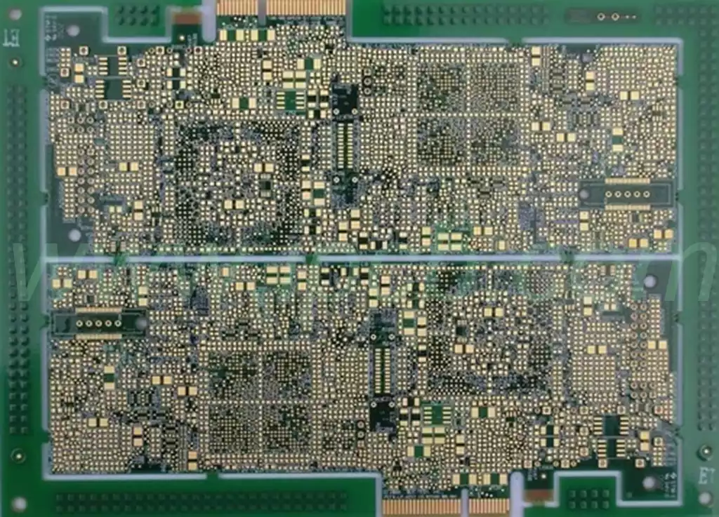
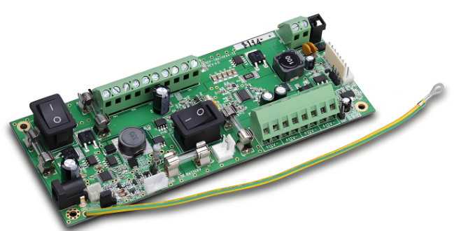
At the core of any electronic device lies a PCB board, a flat sheet composed of insulating material with conductive pathways etched onto it. The primary material used for the substrate is usually fiberglass reinforced epoxy resin (FR-4), which provides mechanical support and electrical insulation. Copper is the most common conductive material used for creating the traces and pads on the PCB board. These traces act as electrical pathways, connecting various components on the board.
A typical PCB board consists of several layers, including:
- Substrate Layer: This is the base material that provides structural integrity.
- Copper Layer: Thin layers of copper foil are laminated onto the substrate and etched to form the conductive traces.
- Solder Mask Layer: This layer covers the copper traces to prevent short circuits and oxidation. It also helps in the soldering process by keeping solder in place.
- Silkscreen Layer: The top layer where component labels, symbols, and other markings are printed to aid assembly and troubleshooting.
Types of PCB Boards
There are several types of PCB boards, each designed to meet specific needs and applications in the electronics industry. The most common types are:
- Single-Sided PCB Boards: These boards have copper traces on one side of the substrate only. They are the simplest and cheapest to manufacture, suitable for low-density designs and straightforward electronic circuits.
- Double-Sided PCB Boards: These boards have copper traces on both sides of the substrate, allowing for more complex circuits and higher component density. They are widely used in consumer electronics, industrial control systems, and automotive electronics.
- Multi-Layer PCB Boards: These boards consist of multiple layers of substrate and copper, laminated together. They allow for highly complex and dense circuit designs, often found in high-performance computing devices, advanced communication equipment, and sophisticated medical devices.
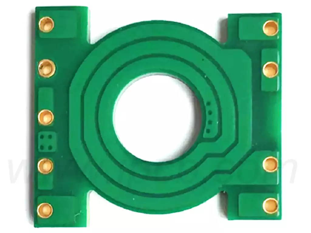
- Flexible PCB Boards: Made from flexible materials like polyimide, these boards can bend and twist to fit into tight or irregular spaces. They are commonly used in wearable devices, flexible displays, and portable electronics.
- Rigid-Flex PCB Boards: Combining rigid and flexible board technologies, these boards offer both flexibility and structural stability. They are ideal for applications that require both rigid and flexible sections, such as in aerospace and military equipment.
Manufacturing Process of PCB Boards
The manufacturing of PCB boards is a meticulous process that involves several key steps to ensure quality and reliability. The main stages include:
- Design and Layout: Using specialized software, engineers create the schematic and layout of the PCB board, specifying the placement of components and routing of traces.
- Material Preparation: The substrate material is cut to size and cleaned to remove any contaminants.
- Copper Cladding: A thin layer of copper foil is laminated onto the substrate material.
- Photolithography: A photoresist material is applied to the copper surface, and a mask with the desired circuit pattern is used to expose the photoresist to light. The exposed areas are then developed, leaving behind the circuit pattern.
- Etching: The board is subjected to a chemical solution that removes the unprotected copper, leaving the desired traces and pads.
- Drilling: Holes are drilled into the board for vias and component leads. These holes are then plated with copper to ensure electrical connectivity between layers.
- Solder Mask Application: A solder mask is applied to protect the copper traces and prevent solder bridges during assembly.
- Silkscreen Printing: Labels, symbols, and component outlines are printed onto the board to assist in assembly and troubleshooting.
- Final Inspection and Testing: The finished PCB board undergoes visual inspection, electrical testing, and functional testing to ensure it meets quality standards.
Applications of PCB Boards in Electronics
PCB boards are integral to the functioning of a wide range of electronic devices and systems. Some of the key applications include:
- Consumer Electronics: PCB boards are found in virtually all consumer electronic devices, such as smartphones, tablets, laptops, televisions, and gaming consoles. They provide the essential framework for assembling and interconnecting various electronic components.
- Industrial Control Systems: In industrial settings, PCB boards are used in control systems, automation equipment, sensors, and other electronic devices. They enable precise control and monitoring of industrial processes, enhancing efficiency and productivity.
- Automotive Electronics: Modern vehicles rely heavily on PCB boards for various electronic systems, including engine control units, infotainment systems, navigation systems, and advanced driver assistance systems (ADAS). These boards ensure reliable and efficient operation of the vehicle’s electronic systems.
- Medical Devices: PCB boards are critical in the medical field, where they are used in diagnostic equipment, monitoring devices, and therapeutic devices. They enable the accurate and reliable operation of medical electronics, contributing to improved patient care and outcomes.
- Telecommunications: PCB boards are essential components in telecommunications equipment, such as routers, switches, modems, and base stations. They provide the necessary infrastructure for transmitting and receiving data, enabling communication networks to function effectively.
- Aerospace and Defense: In aerospace and defense applications, PCB boards are used in avionics, radar systems, communication systems, and other critical electronic systems. They ensure the reliable and robust performance of these systems in demanding environments.
Challenges in PCB Board Manufacturing
Despite their widespread use and critical importance, PCB boards face several challenges that can impact their performance and reliability. Some of the main challenges include:
- Miniaturization: As electronic devices become smaller and more compact, the demand for miniaturized PCB designs increases. This requires advanced manufacturing techniques and materials to create high-density and high-performance boards.
- Heat Dissipation: The increasing power density of electronic components generates more heat, which must be effectively dissipated to prevent overheating and ensure reliable operation. This necessitates the development of advanced thermal management solutions for PCB designs.
- Signal Integrity: High-speed electronic devices require PCB boards with excellent signal integrity to ensure accurate data transmission. This involves careful design and layout to minimize signal loss, crosstalk, and electromagnetic interference.
- Environmental Concerns: The production and disposal of PCB boards can have environmental impacts, including the generation of hazardous waste and the consumption of natural resources. There is a growing emphasis on sustainable manufacturing practices and the development of eco-friendly materials for PCB production.
- Cost Management: Balancing the need for high-quality PCB boards with cost constraints is a constant challenge. Manufacturers must find ways to optimize their processes and materials to deliver cost-effective solutions without compromising on quality.
Future Trends in PCB Board Electronics
The field of PCB board electronics is continually evolving, driven by advancements in technology and changing market demands. Some of the key trends shaping the future of PCB boards include:
- High-Density Interconnect (HDI) PCBs: HDI PCBs feature finer traces and spaces, smaller vias, and higher layer counts, enabling more complex and compact designs. They are increasingly used in smartphones, tablets, and other portable devices.
- Embedded Components: Embedding passive and active components within the PCB substrate itself can reduce the overall size and improve the performance of electronic devices. This approach is particularly beneficial for high-frequency applications and space-constrained designs.
- Advanced Materials: New materials, such as high-frequency laminates and thermally conductive substrates, are being developed to meet the performance requirements of high-speed and high-power applications.
- Flexible and Stretchable PCBs: Flexible PCBs are evolving to become more durable and capable of withstanding extreme bending and stretching. These advancements open up new possibilities for wearable electronics, medical implants, and other innovative applications.
- Environmental Sustainability: There is a growing focus on developing eco-friendly PCB manufacturing processes and materials. This includes the use of lead-free solder, recyclable substrates, and reducing the environmental impact of chemical processes.
- Integration with Emerging Technologies: The integration of PCB boards with emerging technologies such as 5G, artificial intelligence, and the Internet of Things (IoT) is driving innovation in the electronics industry. These technologies require advanced PCB designs that can support higher speeds, greater functionality, and improved connectivity.
- Additive Manufacturing: Also known as 3D printing, additive manufacturing is poised to revolutionize PCB production by enabling the creation of complex, multi-layer designs with precise material placement. This technique can reduce waste, lower costs, and increase the speed of prototyping and production.
- Nano-Technology: Incorporating nano-materials into PCB design and manufacturing can enhance the performance and durability of electronic devices. Nano-coatings, for example, can provide superior protection against environmental factors, while nano-conductors can improve electrical performance.
Conclusion
PCB boards are the cornerstone of modern electronics, providing the essential platform for assembling and interconnecting electronic components. Their structure, types, manufacturing processes, and applications are fundamental to the functioning of a wide range of electronic devices and systems. Despite the challenges faced by the PCB industry, ongoing advancements in technology and materials promise to drive innovation and improve the performance and reliability of PCB boards. As we look to the future, the continued evolution of PCB board electronics will play a key role in enabling the next generation of electronic devices and systems. By embracing new technologies and sustainable practices, the PCB industry can meet the growing demands of the electronics market and contribute to a more connected and efficient world.