Flexible printed circuit board (Flexible PCB) has become one of the core components of contemporary electronic devices with its lightness and bendability. Flexible PCB is suitable for smart wearable devices, mobile devices, medical instruments and other fields, and has strong application prospects. However, due to the differences in structure and material properties, the impedance control design of flexible PCB is significantly different from that of traditional rigid PCB, especially in high-speed signal transmission, which puts forward higher requirements for accurate impedance calculation. This article will deeply explore the principles and methods of flexible PCB impedance calculation and the key factors that need to be paid attention to in the design.
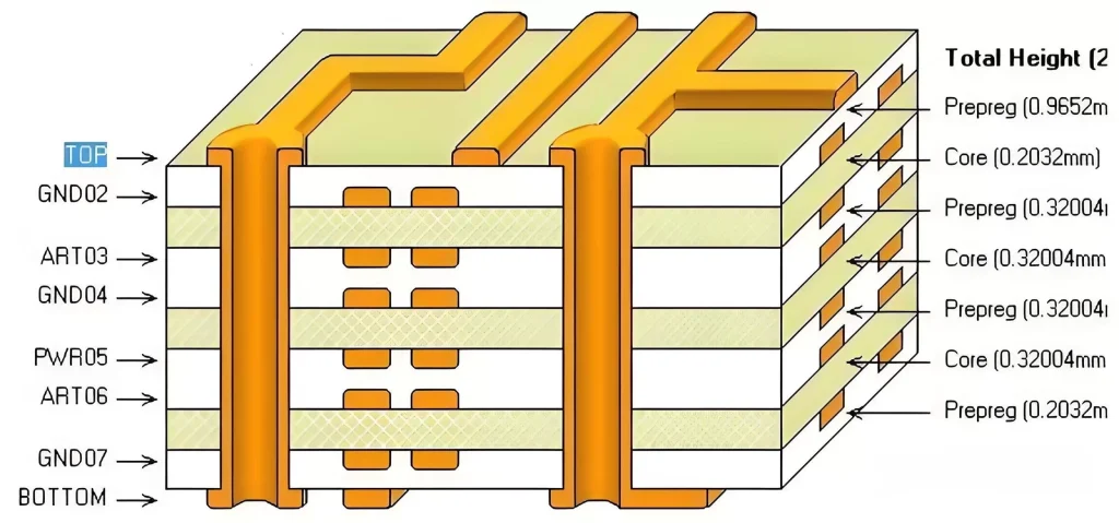
Structure and characteristics of flexible PCB
Flexible PCB consists of copper foil conductive layer, insulation layer and protective layer, etc. The structure of composite material makes it have bending and tensile properties. Unlike traditional rigid PCB, flexible PCB uses flexible materials such as polyimide (PI) or liquid crystal polymer (LCP) as the substrate, which makes it highly flexible and durable while maintaining excellent conductive properties. The key features of flexible PCBs include:
High flexibility: Flexible PCBs have extremely high bending and deformation capabilities, making them suitable for electronic devices that require multiple folding and bending.
Lightness: The thin and light nature of flexible materials makes flexible PCBs more suitable for equipment designs that require weight reduction.
High reliability: Flexible PCBs use heat-resistant and waterproof materials, which can maintain stable performance in harsh environments and avoid deformation or performance degradation at high temperatures.
These features make flexible PCBs an indispensable part of electronic device design. Because they are light and easy to install, flexible PCBs are widely used in wearable devices and industrial automation equipment. The structural design of flexible PCBs requires not only high electrical performance, but also ensures the stability and durability of the circuit in different environments and dynamic bending.
Impedance control requirements for flexible PCBs
In flexible PCBs, impedance control is critical to the quality and integrity of signal transmission. In order to achieve the desired signal transmission effect, different types of impedance control are usually used for different signal characteristics:
Single-ended impedance: Mainly used in lines that transmit a single signal, it has an important impact on the transmission speed, reflection and distortion of the signal. Single-ended impedance control is particularly important in high-frequency signal transmission.
Differential impedance: Mainly used for paired signal line transmission, it has strong anti-interference performance and can significantly improve the transmission reliability of signals. Differential impedance design is usually used in applications such as communication equipment and data centers that have high requirements for signal stability.
Impedance control is particularly important for the signal integrity of flexible PCBs. When designing flexible PCBs, engineers will adjust parameters such as trace width, material thickness, and dielectric constant according to specific application requirements to achieve the required impedance value. These factors are directly related to the transmission quality of the signal. Especially in the scenario of high-speed signal transmission, controlling impedance helps to avoid signal reflection and loss and ensure the accuracy and stability of data transmission.
Principle of impedance calculation of flexible PCBs
In flexible PCBs, the calculation of impedance is mainly based on the principle of electromagnetic field. Usually, designers will calculate the impedance value based on different trace structures, combined with parameters such as the dielectric constant of the material, the thickness of the conductor, and the thickness of the insulation layer. The impedance control of flexible PCBs mostly adopts the following two structural forms:
Microstrip line structure: Microstrip line is a signal transmission path. The signal routing is arranged on the surface of the flexible PCB, and the insulating material separates it from the ground layer. This structure is suitable for the design of surface routing, because the signal is directly transmitted on the surface of the PCB and is less affected by the material and environment.
Stripline structure: Stripline is used for the inner layer routing of flexible PCBs. The stripline structure places the signal transmission path inside the flexible PCB and is usually more common in multi-layer PCBs. The signal transmission path of the stripline structure is affected by the material and multi-layer structure, so it is more suitable for complex and high-density signal transmission scenarios.
These two structures are widely used in different flexible PCB designs. Designers will choose the appropriate structure according to the performance requirements of the specific circuit, and through impedance calculation and simulation testing, ensure that the signal can be stably transmitted at the specified impedance value. The impedance values of microstrip and stripline are directly affected by the PCB material, thickness, and signal path width, so repeated tests are required in the design to achieve the desired impedance control effect.
Key factors to note in flexible PCB impedance calculation
Impedance calculation is not just the application of calculation formulas. It needs to be combined with multiple parameters in actual application scenarios and comprehensively considered to ensure that the impedance of flexible PCB meets the design requirements. The following are several key factors:
Accurate control of dielectric constant
Flexible PCB mainly uses polyimide (PI) or liquid crystal polymer (LCP) as insulating materials. The dielectric constants of these materials vary with frequency. When high-frequency signals are transmitted, small fluctuations in dielectric constants may cause impedance deviations. Therefore, materials with stable dielectric constants need to be selected to ensure accurate control of impedance. In high-speed transmission scenarios, flexible PCB design needs to comprehensively consider the frequency response characteristics of dielectric constants to avoid high-frequency signal distortion.
Conductor thickness and width
Conductor thickness and width are key parameters in flexible PCB impedance calculation. Increasing conductor width will reduce impedance value, while increasing conductor thickness may cause signal transmission loss. For different signal frequencies, the width and thickness of the conductor are also designed differently. In high-frequency signal applications, the design of the thickness and width of the conductor directly affects the accuracy of the impedance, so it is necessary to find the appropriate conductor size through calculation and simulation to match the needs of signal transmission.
Stability of dielectric thickness
The dielectric thickness has a great influence on the impedance, especially in the multi-layer design of flexible PCB, the dielectric thickness tolerance will affect the stability of signal transmission. For this reason, designers usually choose materials with stable thickness and small fluctuations to ensure design consistency. During the manufacturing process, strict control of dielectric thickness can ensure the high consistency of flexible PCB products, thereby improving the product yield and meeting the needs of mass production.
Ambient temperature and humidity
During the use of flexible PCB, changes in ambient temperature and humidity may affect the impedance value. Flexible materials are prone to deformation in high temperature and high humidity environments, resulting in changes in the geometry of the signal transmission path. Therefore, in the impedance control design, the environmental adaptability of flexible materials needs to be considered. In some high-temperature application scenarios, designers will choose high-temperature and moisture-resistant materials to make flexible PCBs to ensure stable operation of the equipment in different environments.
Tools and software for flexible PCB impedance calculation
In order to calculate the impedance of flexible PCBs conveniently and accurately during the design stage, designers usually use special software tools. The following are several commonly used impedance calculation software:
1.Polar Si9000: This is an impedance calculation and simulation tool, which is mainly used to calculate the impedance of microstrip and stripline structures. It is widely used in the PCB design industry, especially for the design of flexible PCBs.
2.Keysight ADS: A powerful electromagnetic simulation tool that can simulate the impedance characteristics of flexible PCBs. It is particularly suitable for high-frequency applications and can accurately simulate complex signal transmission lines.
3.Ansys HFSS: Supports three-dimensional electromagnetic simulation and can accurately simulate the impedance changes of flexible PCBs in complex electromagnetic environments.
These tools can not only help designers quickly calculate impedance, but also provide simulation results to provide data support for impedance control design. Designers can use software to iteratively adjust and optimize the design to avoid signal problems caused by impedance deviation. Impedance simulation software can minimize errors in the design process and make the impedance control of flexible PCBs more accurate.
Practical cases of flexible PCB impedance calculation
In practical applications, flexible PCB impedance control design is often used in smart wearable devices. Flexible PCBs in these devices not only require efficient signal transmission, but also need to withstand multiple bending and folding tests. Therefore, in actual design, designers will use materials with high durability and low impedance deviation, and use electromagnetic simulation software for impedance calibration to ensure the stability and reliability of the product.
For example, in the flexible PCB design of a smart watch, the designer implemented single-ended impedance control through a microstrip line structure to ensure stable transmission of signals between the screen and the processor. In actual tests, the impedance control accuracy of the flexible PCB met the design standards, allowing the signal transmission of the smart watch to remain efficient and reduce signal distortion and reflection.
Future trends in flexible PCB impedance design
With the popularization of flexible electronic devices, the impedance control technology of flexible PCBs is also developing. Future flexible PCB impedance design will focus more on:
Precise material control: With the development of material science, low-loss materials that adapt to higher frequencies may appear in the future, further improving the impedance control ability of flexible PCBs.
Smarter design software: Future software may integrate AI algorithms to automatically optimize impedance design by learning design patterns, shorten design cycles and improve accuracy.
Multi-layer flexible PCB technology: As demand increases, the design difficulty of multi-layer flexible PCBs will increase, and more accurate impedance control will be required in the future to meet the needs of multi-layer complex signal paths.
These trends will play a key role in the field of impedance design of flexible PCBs, providing support for the miniaturization and lightness of electronic devices.
Conclusion
The impedance calculation of flexible PCBs is a system engineering with multi-factor coordinated control, involving materials, processes, design and other aspects. Through accurate impedance calculation, designers can ensure the signal integrity and anti-interference ability of flexible PCBs in practical applications. With the increasing demand for miniaturization and lightweight electronic devices, the impedance design of flexible PCBs will continue to develop and provide more efficient solutions for high-performance electronic devices.
This article summarizes the basic principles, calculation methods and key points of flexible PCB impedance control. I hope that this article will help you understand the impedance design of flexible PCBs and help you achieve higher quality flexible PCB designs.
