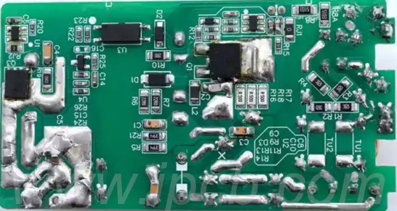
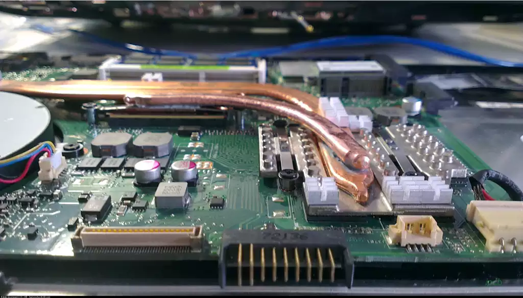
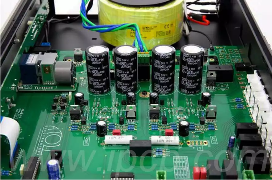
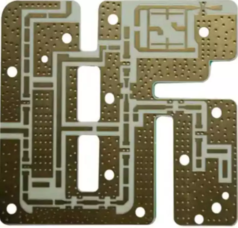
In today’s digital age, USB hub circuit boards have become a key component for connecting multiple devices. With the continuous advancement of technology, users’ growing demand for data transmission speed, number of interfaces and device compatibility has promoted the rapid development of USB hub circuit boards.

Basic concept of USB hub pcb board
The main purpose of USB hub circuit boards is to expand a single USB interface into multiple independent ports, allowing users to connect multiple external devices at the same time, such as keyboards, mice, USB flash drives, mobile hard drives, printers, etc. Its core advantage is to improve device connection efficiency and reduce repeated plugging and unplugging operations, which is particularly important today when laptop interfaces are decreasing.
In addition, with the diversification of USB interface types, such as Type-A, Type-B, Micro-USB, USB-C, etc., USB hub circuit boards also need to design flexible interface combinations to adapt to the use scenarios of different terminal devices. This not only tests hardware design capabilities, but also poses new challenges to the shell structure and heat dissipation space.
From a functional perspective, modern USB hub circuit boards are no longer just simple “splitters”, but have advanced functions such as intelligent power supply identification, dynamic power adjustment, status LED indication, hot plug protection, etc., and are a bridge for intelligent communication between systems and peripherals.
Technology Evolution and Standards
Since its launch, USB technology has undergone multiple upgrades from USB 1.1 to USB 3.2. Each upgrade brings higher data transmission rates and stronger power supply capabilities. Modern USB hub circuit boards usually support USB 3.0 or higher standards, providing data transmission speeds of up to 5Gbps or faster, meeting high-bandwidth requirements such as high-definition video transmission and large-capacity data backup.
Design Points and Challenges
In terms of signal integrity design, engineers need to use professional simulation tools such as HyperLynx and SIwave to evaluate the reflection, crosstalk and delay of high-speed signals between different layers in advance. In the case of many wiring layers and dense interfaces, blind buried vias and HDI designs can effectively reduce the board area, but will significantly increase manufacturing costs.
In terms of power management, USB hub circuit boards usually need to design multi-channel LDO (low dropout regulator) or DC-DC converter to power each interface, and cooperate with P-MOS tubes, current limiting resistors, current sensors and other components to achieve overload protection. In some portable scenarios, a battery management module may also be added to achieve power-off battery life.
In terms of compatibility, considering the handshake protocol, startup time, and current peak differences of different USB devices, the “enumeration” strategy of the USB controller needs to be considered during design to quickly identify connected devices and ensure that each port will not be disconnected or fail due to insufficient power.
Application Fields
USB hub circuit boards play an important role in many fields:
Personal computers: expand USB interfaces and connect peripherals such as keyboards, mice, and printers.
Data centers: manage a large number of storage devices and improve data processing efficiency.
Industrial automation: connect various sensors and controllers to achieve automated control.
Medical equipment: connect a variety of medical instruments to improve diagnosis and treatment efficiency.
Future Development Trends
With the popularity of the Internet of Things and smart devices, USB hub circuit boards will face higher performance and reliability requirements. Future development directions may include:
Higher data transfer rates: Support USB 4.0 and higher standards.
Intelligent power management: Dynamically adjust power distribution according to device needs.
Modular design: Easy to maintain and upgrade.
Enhanced security: Prevent unauthorized device access.
Chip solutions and control logic in USB hub circuit boards
The core function of the USB hub circuit board depends on its internal control chip, which plays the role of “diversion command”. Common USB hub chip manufacturers include VIA Labs, Microchip, Genesys Logic, Texas Instruments, etc. Chips from different manufacturers vary in interface compatibility, power management capabilities, maximum number of ports supported, power consumption control, etc. Design engineers need to make appropriate choices based on the final product positioning.
For example, some high-performance hub chips support USB BC 1.2 charging protocol, which can not only communicate data, but also provide fast charging capabilities for mobile devices. This type of chip has a dynamic switching function. When the host is detected to be offline, it can switch to an independent power supply mode to continuously power peripheral devices. High-end chips even support the USB-C PD protocol, which can provide bidirectional power supply between the laptop and the docking station.
In terms of control logic, the circuit board needs to design corresponding timing control and power-on logic to ensure that multiple USB devices can be correctly identified when connected and no resource conflicts occur. In addition, some chips also support communication with the host through I²C or SPI bus, which is suitable for scenarios that require remote management in embedded devices or industrial-grade systems.
Anti-interference and electromagnetic compatibility design
USB hub circuit boards are easily affected by the external environment in actual work, especially in data-intensive or electromagnetic noise environments. In order to ensure data transmission stability and interface response speed, anti-interference design (EMI) and electromagnetic compatibility (EMC) have become important links that cannot be ignored.
First, in the PCB wiring stage, the equal length layout of differential signal pairs (such as D+ and D-) should be used as much as possible to avoid signal timing mismatch. At the same time, in order to reduce signal reflection, impedance matching should be reasonably controlled, especially in high-speed applications of USB 3.0 and above, the line width, trace spacing, and stacking structure must be precisely calculated.
Secondly, common-mode inductors and TVS diodes can be installed around the USB port. These devices can effectively absorb surge voltage and reduce the damage caused by electrostatic shock. At the same time, the port is designed with a ground loop to avoid the formation of stray loops and enhance system stability.
The shielding layer design is also very important, especially in the USB hub with a metal shell. The connection between the metal shell and the ground layer forms an overall shielding cage to suppress electromagnetic radiation. In addition, a reasonable grounding strategy, including single-point grounding and complete ground plane of the whole board, plays a key role in anti-interference.
Testing and verification process of USB hub
In order to ensure that the USB hub circuit board shipped from the factory is stable in actual use, it must pass a series of rigorous testing processes, including functional testing, signal testing, electrical performance testing, pressure and anti-static testing, etc.
Functional testing mainly verifies whether each USB port can identify different types of devices, such as high-speed USB flash drives, low-speed keyboards, mice, etc.; whether it supports backward compatibility with USB 3.0, 2.0 and other protocols; and whether it supports simultaneous reading and writing of multiple ports.
Signal testing uses an oscilloscope to analyze the eye diagram, jitter, delay and other indicators of USB data transmission to ensure that there is no code loss under high-speed transmission. For industrial-grade products, environmental stress tests such as high-temperature aging, vibration testing, and salt spray testing will also be introduced to verify long-term operating reliability.
In addition, in order to meet the requirements of EMC/EMI regulations, it is also necessary to pass the certification of third-party organizations, such as FCC, CE, RoHS, etc., to ensure that electromagnetic radiation and environmental pollution are within the specified range, so as to facilitate export to the global market.
Market application status and localization trend
With the improvement of the performance of domestic chips and controllers, more and more core components of USB hub circuit boards have been transformed from imported to domestic solutions. For example, domestic manufacturers such as GigaDevice, Hangshun, and Unisplendour Tongxin have launched a number of stable USB control chips that support 3.0 and above protocols, and have obvious advantages in terms of cost, performance, and supply cycle.
In terms of the terminal market, in addition to traditional consumer electronics products, the application of USB hub circuit boards in industrial control, automated factories, smart medical care, and educational informatization is also expanding. For example, in the operating room, multiple surveillance cameras, operation panels, and display screens need to be connected to the central computing system through a USB hub; in a smart classroom, multiple touch panels, wireless receivers, and recording and broadcasting equipment also need to rely on USB hubs for efficient management.
In the future, with the continuous improvement of domestic manufacturing levels, China’s USB hub circuit boards will not only be more competitive in price, but will also continue to make breakthroughs in reliability and innovation, providing more high-quality choices for the global market.
The combination of USB hub circuit boards and embedded systems
Embedded systems are widely used in smart devices, vehicle terminals, security systems, and IoT edge nodes. The USB hub circuit board serves as a key bridge connecting these embedded platforms with external input and output devices. In this type of application, in addition to conventional data communication functions, energy consumption control, small size design, interface stability and other requirements must also be considered.
For example, on an NVR device in the security field, multiple USB storage devices are often required to be connected for local video backup. At this time, a USB hub circuit board that supports USB 3.0 high-speed interface, has a metal shielding shell and a self-recovery fuse becomes an ideal solution.
In the vehicle system, the USB hub not only serves the entertainment system, but also can interact with diagnostic tools, firmware upgrade tools, and GPS receiving modules for data exchange. Therefore, it is necessary to support anti-seismic design, high and low temperature working ability, and long-term operation stability.
Summary
As an indispensable connection hub in modern electronic devices, the USB hub circuit board has gradually developed from the initial basic expansion function to a comprehensive module with high-speed transmission, intelligent power supply, strong compatibility and multiple protection mechanisms. In practical applications, it widely serves multiple fields such as consumer electronics, industrial control, smart home, and vehicle systems. With the rise of domestic chips and the continuous advancement of technology, the design of USB hub circuit boards is more flexible, the performance is stronger, and the cost is better, and it will play a more important role in the future smart hardware ecosystem. For hardware engineers, mastering the key design points, circuit principles and testing methods is not only the key to improving product competitiveness, but also the basis for gaining a foothold in the ever-evolving electronic world.


