Process principles and differences between SAP and mSAP
In traditional PCB manufacturing, the most commonly used method is the subtractive process, which is to remove unnecessary copper from the entire copper-clad board by etching to form the required circuit pattern. This method performs well when the line width is greater than 100μm, but when the design requirements require the line width and spacing (L/S) to be less than 50μm or even 30μm, the subtractive process gradually exposes its limitations in precision control, etching alignment, and copper wire side etching.
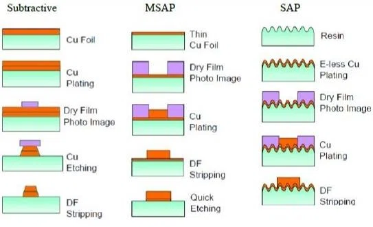
In order to solve this problem, the industry began to adopt the SAP (Semi-Additive Process) process. The idea of SAP is to “form the circuit structure first, and then thicken it by electroplating”. The core steps include:
First, a very thin seed copper layer is deposited on the copper-clad substrate;
Then a photolithography process is used to form a pattern in the required circuit area;
Then electroplating is performed in these areas to thicken to the target circuit thickness;
Finally, the photoresist is removed and the seed copper layer that has not been thickened by electroplating is etched away to retain the copper wire.
This method greatly improves the accuracy and edge smoothness of the circuit pattern and reduces the occurrence of side erosion.
mSAP (Modified Semi-Additive Process) is a refined process further optimized on the basis of SAP. In the specific implementation, mSAP cancels the initial overall copper foil layer, directly deposits a very thin seed copper on the insulating medium, and then forms the pattern and electroplates it, and finally removes the excess part. The biggest advantage of this is that it can achieve finer line widths and spacings, such as 15μm/15μm, or even 12μm/12μm design requirements, greatly improving the wiring density, and is widely used in smartphone motherboards, RF modules, camera modules, and high-frequency packaging.
From a technical point of view, SAP is suitable for designs with line widths between 30–50μm, while mSAP can meet the needs of higher density and smaller size products, especially for high-end consumer electronics. Both represent the core level of current high-density interconnect technology, and are evolving towards lower line widths and more layers.
Detailed analysis of the manufacturing process
Whether it is SAP or mSAP, as representative processes of high-density interconnection, they involve complex and highly precise manufacturing processes. Understanding these processes not only helps to evaluate supplier capabilities, but also helps procurement personnel identify the core key points of product quality.
Brief description of SAP process flow
The SAP process is based on a combination of subtractive and additive methods. The main processes are as follows:
Substrate preparation: Select a suitable substrate (such as ABF resin, BT resin, PI, etc.), which usually requires good dimensional stability and electrical properties.
Seed copper deposition: Deposit a very thin seed copper layer (generally 0.1μm~0.3μm thick) on the entire substrate surface to lay the foundation for subsequent electroplating.
Photolithography: Apply dry film or liquid photosensitive resin, and after exposure and development, form the required circuit pattern.
Graphic electroplating: Electroplating is performed in the exposed copper area after development to make the copper wire thickness reach the designed value (for example, 8~15μm).
Stripping and etching: remove the photoresist and etch away the seed copper that has not been thickened by electroplating, leaving a copper circuit with fine graphics.
Repeated lamination and alignment: For multi-layer boards, the above process needs to be repeated and precise inter-layer alignment is performed, often in conjunction with laser drilling and chemical plating.
Surface treatment: For example, immersion gold, OSP, immersion silver, etc., select the appropriate surface coating according to the final assembly requirements.
mSAP process flow details
Although the mSAP process has many similarities with SAP, it is more suitable for ultra-high density and ultra-fine circuit manufacturing. The key difference in its process is mainly reflected in the initial copper deposition and graphic construction method:
Direct deposition of copper seed layer: mSAP generally does not use traditional copper clad laminates, but directly deposits an ultra-thin seed copper layer on the surface of the insulating layer by chemical methods, avoiding the line width control risk caused by copper etching.
High-resolution lithography: Use higher-precision exposure equipment (such as laser direct writing, stepper exposure machine) for imaging, the edges of the graphics are clearer, and it is suitable for finer spacing.
Fine plating and copper thickness control: After plating, the copper thickness control is more precise, usually maintained below 10μm, to reduce the volume and improve signal integrity.
Plasma or dry etching to remove the copper layer: mSAP uses more advanced dry processing technology to avoid pattern damage caused by wet corrosion.
High-density multi-layer interconnect integration: Complex signal layer stacking is achieved through buried holes, blind holes and any layer interconnect.
Manufacturing challenges of mSAP and SAP
The SAP process has certain challenges in controlling the edge roughness of copper wires and etching consistency;
mSAP places extremely high requirements on deposition accuracy, exposure resolution, photoresist quality, etc.;
Both have high standards for cleanliness, temperature control, alignment system, etc., which is a comprehensive test of the entire production line equipment and personnel technical capabilities.
In summary, although SAP and mSAP belong to the same technology family, they have obvious stratification in terms of accuracy, process complexity and equipment requirements. Especially when dealing with high-frequency signals, high-density wiring, and small-size chip packaging, mSAP has become the mainstream in the industry.
Key technical advantages and challenges
The reason why mSAP and SAP processes have risen rapidly in the field of high-density interconnection and become the first choice of many leading electronic product manufacturers is that they have shown technical advantages that traditional subtractive processes cannot match in terms of circuit accuracy, wiring density, signal integrity, etc. However, the more sophisticated the process, the higher the requirements for materials, equipment, environment, and technology, and it also brings a series of practical challenges.
Technical Advantages Analysis
Higher Wiring Density
The traditional subtractive method is limited by etching accuracy and it is difficult to achieve a line width/line spacing of less than 50μm, while the SAP process can control the line width to about 30μm, and mSAP can reach 15μm, or even below 12μm, which greatly increases the number of signal wiring per unit area. This is particularly critical for highly integrated scenarios such as smartphone motherboards, camera modules, and RF chip packaging.
Superior signal integrity
The smaller line width and line spacing combined with precise control of copper thickness enable signals to have lower crosstalk, less reflection and better impedance matching during high-frequency and high-speed transmission. Especially when dealing with scenarios such as 5G high-frequency signals and AI high-speed data transmission, the fine line layout of mSAP significantly improves the overall electrical performance.
Smaller product size
Through the combination of extremely small line width and arbitrary layer interconnection, equipment manufacturers can integrate more functional modules in a smaller space to achieve miniaturization and thinness of terminal products. This is also one of the technical foundations for modern mobile phones to become thinner and more functional.
Higher yield consistency
Because the mSAP process has lower edge roughness and more consistent copper deposition thickness, it shows higher consistency in mass production, with small differences between products, thereby reducing the rework rate of back-end assembly and saving comprehensive manufacturing costs.
Practical challenges and technical bottlenecks
Imaging resolution limitations
mSAP places extremely high demands on the resolution of the lithography system, and traditional exposure methods (such as mask alignment) are difficult to meet the requirements. Therefore, most manufacturers need to introduce expensive laser direct writing or stepping exposure equipment, which greatly increases capital investment.
Material compatibility and interface adhesion
The seed copper layer is directly deposited on the insulating medium. If the interface is not properly treated, problems such as copper wire peeling or electromigration failure may occur, affecting long-term reliability. Especially in multi-layer stacked structures, inconsistent thermal expansion coefficients between layers may also cause deformation or delamination.
Narrow etching and electroplating process window
mSAP has very high control accuracy requirements for the thickness of the copper layer. A slight deviation may cause line breakage or short circuit. At the same time, process defects such as photoresist residue, uneven development, and chemical treatment residue may cause graphic distortion, and process parameters need to be continuously optimized.
Cost pressure and yield game
Although mSAP brings significant electrical and structural advantages, its manufacturing cost is high and its tolerance for process control is low. In the early batch introduction stage, it often faces the problems of slow yield ramp-up and high rework costs. How to reduce the cost of single boards while ensuring quality is an important issue facing enterprises.
Key directions in continuous optimization
Improve the resolution of the exposure system and advance to EUV lithography or micro-wave direct writing;
Introduce plasma cleaning technology to improve interface cleanliness and adhesion;
Achieve full-process data monitoring and deviation warning through MES+AI;
Develop new photoresist and seed copper alternative materials suitable for mSAP to improve ecological compatibility.
Core application areas
As advanced high-density interconnect solutions, mSAP and SAP technologies have been widely used in many core areas of the electronics industry, promoting a leap in product performance and functionality. Understanding these typical applications not only helps technicians understand the value of the process, but also allows purchasers and customers to see actual market demand and future trends.
Smartphone motherboards and RF modules
As an indispensable communication device for modern people, smartphones have extremely high requirements for the integration and performance of motherboards. With its fine line width and excellent signal integrity, the mSAP process has become an ideal choice for manufacturing high-speed signal lines and RF transmission paths on motherboards.
RF modules are extremely sensitive to the transmission loss of high-frequency signals. The roughness of the lines and irregular edges of the traditional subtractive process can easily lead to signal reflection and interference, seriously affecting the signal quality. mSAP high-precision lines reduce signal loss, improve the sensitivity and stability of the module, and support the performance requirements of 5G, WiFi 6 and higher frequency band communications.
Camera modules and micro sensors
With the improvement of mobile phone camera functions and the rise of autonomous driving and smart security, the size of camera modules and various micro sensors is getting smaller and smaller, and the wiring density is rising. The ultra-fine line capability of mSAP can achieve high-density signal interconnection within the module to ensure high-speed and stable image transmission.
In addition, micro sensors have extremely high requirements for reliability and signal accuracy. mSAP’s good copper wire uniformity and thickness control avoid signal attenuation and circuit breakage, greatly improving the stability and life of terminal products.
High-performance computing and data center equipment
In data centers and servers, the layout of high-speed signal and power management lines is particularly critical. SAP and mSAP technologies are applied to high-end PCBs and package substrates to provide stable electrical connections for chips and modules.
In these devices, the signal rate is extremely high, and any tiny line defects may lead to performance bottlenecks. High-density wiring made with mSAP not only improves signal integrity, but also optimizes the power distribution network, reduces thermal resistance and electromagnetic interference, and ensures long-term stable operation of the equipment.
Automotive electronics and industrial control
As the degree of automotive intelligence continues to increase, the requirements of electronic control units (ECUs) for PCBs are becoming more and more stringent. The mSAP process can meet the needs of automotive electronics for heat resistance, vibration resistance and long-term reliability, and is particularly suitable for manufacturing high-density sensor interfaces and complex control boards.
The industrial control field also requires high reliability and high-density interconnection. mSAP, with its excellent process stability, helps equipment achieve more complex functional integration and more compact design.
Quality control and manufacturing difficulties
Although high-density interconnection technologies such as SAP and mSAP bring many advantages, due to the complex process and numerous manufacturing links, quality control has become the key to ensuring product performance and yield. The following will analyze in detail the common difficulties in manufacturing and the corresponding quality management measures.
Lithography and graphic precision control
Lithography is the core process step of SAP and mSAP, and its success or failure directly determines the accuracy and precision of the circuit. During the lithography process, parameters such as exposure dose, development time, and temperature must be strictly controlled to prevent distortion, edge burrs, or overexposure of the graphics.
Advanced lithography equipment, such as laser direct writing systems or stepper exposure machines, have higher resolution and can effectively avoid graphic distortion. However, the equipment maintenance and environmental cleanliness requirements are extremely high. Once particles or chemical residues cause lithography defects, it may cause circuit breakage or short circuits.
Uniformity of seed copper layer deposition
The uniformity and adhesion of the seed copper layer are the basis for ensuring the quality of the subsequent electroplated copper layer. During the deposition process, any unevenness will lead to inconsistent copper layer thickness, resulting in insufficient local line strength or poor signal transmission.
The chemical deposition process must accurately control the solution concentration, temperature and time to avoid pinholes, voids or peeling. The use of online monitoring technology to adjust the deposition parameters in real time can significantly improve the yield rate.
Electroplating thickness and edge smoothness
The uniformity of the thickness of the electroplated copper layer directly affects the electrical performance and mechanical strength of the circuit. In the mSAP process, the electroplated copper layer is usually thin and requires high precision. Thickness deviation will cause impedance fluctuations and affect the quality of high-speed signals.
In addition, the edge of the electroplated layer must be smooth and burr-free to prevent short circuits or cold solder joints during welding. The current density, stirring rate and temperature must be reasonably adjusted in the process to ensure that the copper layer is densely crystallized and uniform.
Glue and etching process control
After removing the photoresist, the residual colloid must be thoroughly cleaned to prevent residual glue from causing circuit defects. The choice between wet etching and dry etching depends on the circuit design and material properties. Dry etching is more suitable for fine circuits, but the equipment cost is higher.
Any excessive or uneven etching will cause circuit breakage or short circuit. Strict process window control and multiple quality inspection methods (such as automatic optical inspection AOI, X-ray inspection) are necessary conditions to ensure product qualification rate.
Multi-layer alignment and interlayer connection
During the production of multi-layer PCBs, interlayer alignment errors can easily cause abnormal signal transmission. mSAP boards mostly use laser drilling and chemical plating processes to complete interlayer interconnection. It is necessary to ensure that the drilling position is accurate and the copper plating hole wall is uniform.
Improper temperature and pressure control during the lamination process may also cause board warping or interlayer debonding, affecting electrical performance and mechanical strength. Advanced lamination equipment and strict process specifications are the core of ensuring the quality of multilayer boards.
Environmental cleanliness and production management
Since the process is extremely sensitive to tiny particles and chemical residues, the production environment must meet high cleanliness standards. The workshop must be equipped with a high-efficiency filtration system to strictly control humidity and temperature to prevent static electricity accumulation.
At the same time, the use of digital production management systems to achieve real-time monitoring and traceability of process parameters, equipment status and quality data can effectively prevent potential risks and ensure process stability and product consistency.
Future development trends and prospects
As electronic products develop towards smaller, faster, and more multifunctional integration, SAP and mSAP technologies are also evolving, pushing the entire semiconductor packaging and high-density interconnection field to new heights. The following are possible development trends and market prospects for this technology in the next few years.
Finer line width and line spacing
Future product demand for higher integration and smaller volume will drive the SAP/mSAP line width and line spacing to continue to shrink, from the current mainstream 15 microns to 10 microns and below. This requires not only more advanced lithography technology support, but also the combination of new materials and innovative processes to ensure line
Stability and reliability of the circuit.
Application and optimization of new materials
In order to adapt to higher signal frequencies and more complex thermal management requirements, SAP/mSAP substrates will use substrates and copper-clad materials with lower dielectric constants and higher thermal conductivity in the future. At the same time, green environmentally friendly materials and lead-free processes will also become industry standards to promote sustainable development.
Intelligent manufacturing and automation upgrade
Combined with the concept of Industry 4.0, SAP/mSAP production lines will be more intelligent. Through big data analysis, machine learning and automated testing, the whole process from design, manufacturing to quality inspection can be optimized. Smart factories can respond to market changes faster, improve yields and reduce costs.
Deep integration with advanced packaging technology
SAP and mSAP will be further combined with advanced packaging technologies such as wafer-level packaging (WLP) and system-level packaging (SiP) to form a complete high-density interconnection solution. Especially in emerging fields such as 5G communications, artificial intelligence and the Internet of Things, it meets the needs of high-speed data transmission and complex functional integration.
Balance between cost and scale
Although the manufacturing cost of mSAP technology is relatively high, with the upgrading of equipment, the maturity of process and the emergence of scale effect, the cost is expected to continue to decline in the future. Supply chain integration and process standardization will also help enterprises achieve large-scale production and promote the popularization of technology.
Summary
As core technologies in the field of high-density interconnection, SAP and mSAP have become indispensable manufacturing processes in many industries such as smartphones, high-frequency communications, and automotive electronics with their excellent line accuracy and excellent electrical performance. They not only promote the miniaturization and functional diversification of electronic products, but also provide a solid foundation for high-speed signal transmission and complex system integration.
Faced with the challenges of complex processes, high equipment requirements and high manufacturing costs, the industry continues to improve process stability and production efficiency through technological innovation and intelligent manufacturing. In the future, with the continuous integration of new materials, advanced lithography and automation technologies, SAP and mSAP technologies will maintain rapid development, helping the electronics industry to usher in a new era of smarter, faster and more environmentally friendly.