With the development of cutting-edge technologies such as 5G, artificial intelligence, and the Internet of Things, electronic products have put forward higher requirements for high-frequency, high-speed, low-loss, and low-dielectric circuit materials. In this context, traditional materials such as epoxy resins, ceramics, and polyimides are facing performance bottlenecks, and glass PCBs, as an emerging high-performance material, are gradually gaining attention in the field of electronic manufacturing.
Although glass PCBs have not yet become mainstream in practical applications, their potential in high-end fields such as communications, automobiles, and medical care cannot be ignored. This article will deeply analyze the core value of this new material from five dimensions: basic definition, technical advantages, manufacturing challenges, application fields, and future trends.
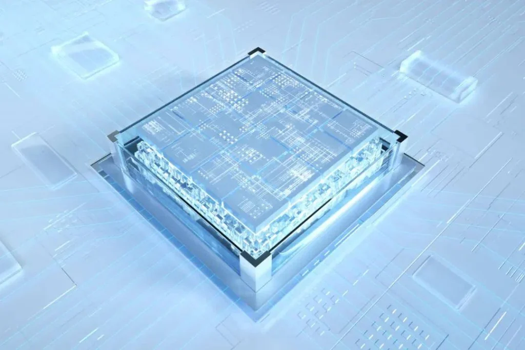
What is glass PCB?
Glass PCB is a form of printed circuit board with glass as the substrate. It is different from the traditional FR-4 substrate. Its material essence is a glass plate with high purity and low thermal expansion coefficient. This type of PCB usually has excellent electrical insulation, thermal stability, and mechanical strength, and is suitable for some extreme environments and application scenarios with extremely high performance requirements.
Glass PCBs are generally made of soda-lime glass, borosilicate glass or quartz glass, combined with fine line processing technology and metal layer deposition technology to form a solderable and mountable conductive structure. Due to the rigidity and transparency of its substrate, it is also commonly used in transparent electronics, sensors and optoelectronic devices.
Technical advantages of glass PCBs
Extremely low dielectric loss
The dielectric constant (Dk) of the glass material itself is low and has good frequency stability. This has a natural advantage for high-frequency signal transmission, especially for millimeter wave communications, radar systems and other fields, which can effectively reduce signal attenuation and crosstalk and improve data integrity.
Excellent thermal stability
The thermal expansion coefficient of glass is very small (CTE < 1ppm/°C), which can adapt well to high temperature environments, and is of great benefit to the stability of BGA and chip welding structures. Compared with organic materials, it is not easy to deform or delaminate under high temperature conditions, which helps to improve the reliability of packaging and systems.
High mechanical strength and dimensional stability
Glass has good bending and compression resistance, especially when maintaining ultra-thin thickness, it can still maintain high strength. This makes it more stable when manufacturing large-size, high-precision PCBs, and is suitable for use in precision electronic systems that require extremely high geometric tolerances.
Optical transparency and packaging integration potential
Some glass substrates have excellent optical properties and can transmit visible and infrared light, making them suitable for emerging applications such as optoelectronic interconnection systems, transparent sensors, and LED lighting substrates. In addition, their surface treatment compatibility is good and suitable for a variety of packaging forms, including Flip Chip, SiP, etc.
Difficulties in the manufacturing process of glass PCBs
Although glass PCBs have many advantages, their manufacturing process also faces a series of challenges, especially in the following aspects.
Brittle processing of glass materials
Unlike metals or plastics, glass is a brittle material and is prone to cracks or edge collapse during processing. Traditional drilling or cutting tools often cannot meet the needs of high-precision non-destructive processing, so advanced processes such as laser processing and ultrasonic assistance are required, which places extremely high demands on equipment and increases manufacturing costs.
The metal layer deposition process is complicated
Glass itself cannot be directly metallized like FR-4, so its surface must be specially treated (such as sputtering, magnetron deposition, etc.) before forming a conductive layer through chemical plating and electroplating. The whole process requires extremely high cleanliness and adhesion control, otherwise poor conduction or peeling is likely to occur.
Welding and packaging compatibility issues
The glass surface does not have natural wettability, so it is easy to desolder and cold solder joints during solder paste printing and chip packaging. In order to improve the reliability of mounting, further surface treatment is required on the metal layer, such as immersion gold, OSP, etc., which increases the complexity of the process.
Batch manufacturing yield control is difficult
At present, glass PCB has not yet formed a large-scale standardized production system, and its yield is mainly affected by factors such as processing micro-cracks, interlayer adhesion, and metal transfer. In the absence of mature experience and data accumulation, it is difficult to achieve high-yield, low-cost mass production.
The laser technologies currently widely used in glass PCB processing include UV Laser and Femtosecond Laser. Among them, femtosecond laser has little thermal impact on materials due to its “cold processing” characteristics, can achieve extremely small apertures, high-precision cutting, and avoid thermal cracks. It is the mainstream means of drilling and cutting micron-level glass in the industry. Especially in the processing of micro vias and through holes, its processing consistency and edge quality play a key role in yield.
Expansion and layout of application fields
Although glass PCB is still an emerging material, there have been cases of landing applications in several high-end fields.
High-frequency communication equipment
In products such as 5G millimeter wave communication base stations and antenna arrays, the demand for PCBs with low loss and stable frequency response continues to grow. Glass PCB has become an important choice for such systems with its ultra-low dielectric loss and high stability.
Optoelectronics and transparent display technology
Transparent conductive circuits combined with glass substrates can be widely used in terminal devices such as AR glasses, HUD head-up displays, photoelectric sensors, etc. that have extremely high requirements for appearance and performance. Its transparency, rigidity, high thermal stability and other characteristics provide unique advantages for such applications.
Medical imaging and sensor systems
In medical imaging processors that require high-precision signal reading and anti-interference capabilities, glass PCBs can provide excellent electrical isolation and dimensional stability, improving system accuracy and safety.
Aerospace and military industry
The extreme requirements for material performance in complex environments have made glass PCBs gradually enter extreme working conditions such as military radar systems and satellite communication modules, and their reliability and environmental adaptability have been valued.
Advantages and challenges compared with traditional PCBs
Performance perspective
Glass PCBs are generally superior to organic materials such as FR-4 in terms of electrical properties, thermal properties, and dimensional stability. Especially in signal transmission above GHz frequency, its advantages are more obvious.
Cost perspective
Currently, the cost of glass PCBs is much higher than that of ordinary PCBs, mainly due to the scarcity of material sources, difficulty in processing, and complex manufacturing processes. However, for products with extremely high performance requirements, its comprehensive cost advantage is gradually emerging, especially in the high-end market segment.
Environmental protection and sustainability perspective
Compared with resin materials, glass can be recycled at high temperatures, is environmentally friendly, has no organic solvent volatilization, and has natural advantages in carbon emissions and material recycling.
Future development trends
The promotion of glass PCB still faces technical barriers and cost control challenges, but with the continuous development of semiconductor packaging technology and laser processing technology, as well as the sharp increase in the industry’s demand for high-frequency and high-speed signal transmission, the following development directions are expected to emerge in the future:
Industry chain integration and standardization: One of the keys to promoting glass PCB into mass production is to establish a complete and replicable process standard system.
Breakthrough in micron-level processing capabilities: The composite processing solution of laser + precision machinery will greatly improve the structural accuracy and reliability of glass substrates.
Enhancement of packaging-level integration capabilities: Combined with advanced packaging such as SiP and Fan-out, glass PCB will play a greater role in system-level integration.
Cost structure optimization: Through material optimization, manufacturing automation and yield improvement, the cost of glass PCB is expected to drop by more than 30% in the future.
At present, the international glass PCB market is dominated by Japan and Germany, but many domestic PCB manufacturers and university research institutes are actively promoting the localization of glass substrate materials. For example, some companies have achieved independent research and development of glass PCB laser drilling equipment and metallization processes, laying the foundation for breaking the monopoly of foreign equipment and reducing overall manufacturing costs. In the future, with policy support and technological accumulation, the maturity of glass PCB in the domestic manufacturing system will steadily increase, and it will also provide more cost-effective options for overseas customers.
Summary
As a new material that is still in the exploration and growth stage, glass PCB has shown great potential in electrical performance, thermal stability, and transparent properties. Although its manufacturing is still facing technical barriers and cost pressure, it has begun to show competitiveness in high-end fields such as high-frequency communications, optoelectronic interconnection, and transparent electronics.
With the continuous breakthroughs in key technologies such as materials science, micro-nano processing, and surface treatment, glass PCB is expected to become the core carrier of the next generation of high-performance electronic systems. For electronic manufacturing companies, early layout of glass PCB is not only a reflection of technological leadership, but also a key competitive advantage in future industrial upgrading.