Introduction
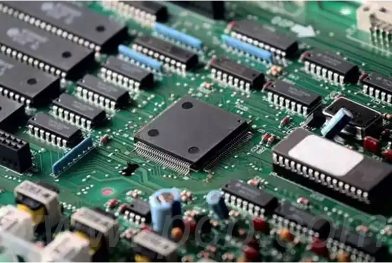
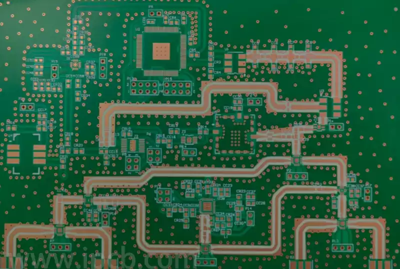
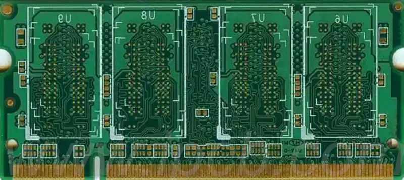
As electronic devices increasingly move toward higher density, higher performance, and smaller form factors, the manufacturing requirements for printed circuit boards (PCBs) are also increasing. As the foundation of electronic systems, the stability and reliability of PCB processes directly impact the overall performance of the product. Solder mask, a crucial component of PCB surface treatment, not only provides electrical insulation, pad protection, and chemical resistance, but also directly impacts soldering quality and appearance.
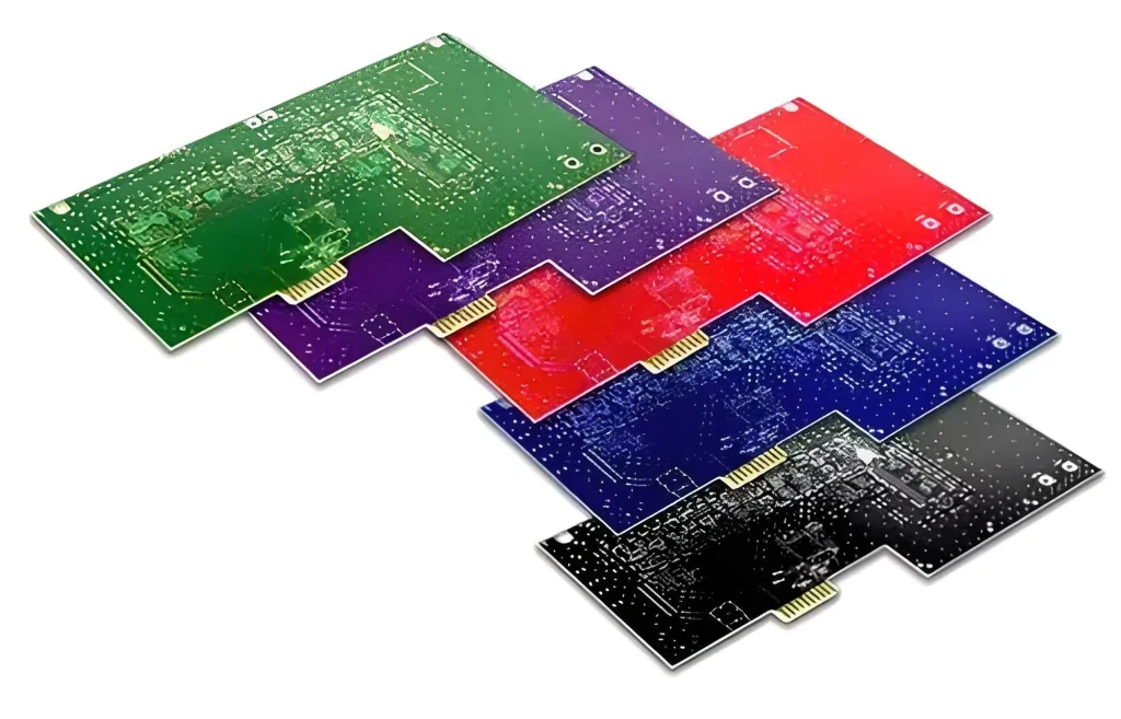
Traditional solder mask applications primarily rely on liquid photosensitive inks. However, with the recent rise of high-precision, high-reliability manufacturing, a new solder mask method—dry film solder mask—has been gaining industry attention and adoption. It offers excellent imaging accuracy, stable film thickness control, reduced contamination risk, and excellent performance suitable for high-end applications. It is gaining popularity in high-value-added products such as HDI boards, IC substrates, and rigid-flex boards.
Despite this, dry film solder mask remains a relatively specialized niche, and many technicians, customers, and procurement personnel still have limited understanding of it, often experiencing misunderstandings and confusion. To this end, this article will comprehensively discuss material principles, manufacturing processes, technical advantages, limitations, application areas, and future developments, helping readers develop a clear and in-depth technical perspective.
What is Dry Film Solder Mask?
Dry Film Solder Mask, also known as Dry Film Solder Mask, is a preformed film material primarily composed of photopolymers. It is applied to PCB surfaces to provide both solder resistance and insulation. Unlike liquid solder mask inks, dry film solder mask is already formed into rolls or sheets at the factory. During use, it is laminated to the PCB surface via heat pressing and then exposed and developed to form a pattern.
Structural Composition
Dry film solder mask typically consists of three layers:
PET protective film: The outermost layer protects the photosensitive layer from contamination and scratches during transportation and storage;
Photopolymer layer: The middle layer, the core functional layer of the dry film, forms the solder mask pattern after exposure;
Bottom release film: Removed before use, allowing the photosensitive layer to be directly applied to the PCB copper surface or dielectric layer.
Principle and Mechanism
Dry film is a positive-acting photopolymer material. After UV exposure, the exposed areas undergo a polymerization reaction, becoming insoluble. Unexposed areas can still be dissolved and washed away with an alkaline developer (such as sodium carbonate solution). After development, the patterned areas remain, while the unpatterned areas expose pads or conductors, facilitating subsequent soldering.
This imaging method uses a similar imaging principle to photoresist, offering inherent advantages in pattern accuracy and linewidth control.
Application Background
Dry film solder mask is not new. Its technology originated in the semiconductor packaging industry in the 1980s and has gradually been applied to high-end PCB manufacturing. It is particularly widely used in the following product categories:
IC substrates: Require extremely stringent control over line width and solder mask window;
High-frequency, high-speed boards: Require low dielectric constant and high surface uniformity;
Rigid-flex boards: Require flexible materials and high-precision processing;
Military/medical electronics: Require stringent reliability and chemical resistance.
Differences Between Dry Film Solder Mask and Liquid Solder Mask
Although both dry film solder mask and liquid solder mask inks are used for solder protection on PCBs, they differ in their process performance, application scope, and finished product appearance.
First, dry film solder mask has a natural advantage in terms of pattern accuracy. Because it uses prefabricated photosensitive film and transfers the pattern through precise lamination and exposure processes, it can achieve higher linewidth control accuracy and edge definition. In contrast, liquid solder mask inks, due to their screen printing or inkjet printing methods, are prone to pattern bleed or blurred edges after exposure, making them unsuitable for extremely high-density designs.
Second, in terms of film thickness control, dry film solder mask, due to its inherently stable thickness, offers far superior overall film uniformity compared to liquid solder mask. Liquid solder mask inks, on the other hand, can experience localized thickness inconsistencies after application due to gravity, fluidity, and the drying process, impacting the flatness and uniformity of the finished product’s solder window.
In terms of process cleanliness, the application of dry film solder mask is relatively cleaner. It eliminates the risk of liquid ink splashing and contaminating equipment or the board surface, and eliminates the need for tedious wiping and cleaning, facilitating dust-free production. Liquid solder mask, however, due to its fluid properties, can easily contaminate the board surface or surrounding environment during the printing process, requiring more controlled processes, especially when used in precision equipment.
Looking at the application scenarios, dry film solder mask is primarily used for products requiring high precision, such as HDI boards, IC carriers, and high-frequency, high-speed boards. It can meet more stringent requirements for pad window control and signal integrity. Liquid solder mask ink, on the other hand, is widely used in general consumer electronics multilayer boards and general-purpose circuit boards, where precision and performance requirements are less extreme.
Finally, in terms of cost and production efficiency, dry film solder mask has relatively high unit and labor costs due to its relatively expensive material, demanding processing equipment, and more complex overall process flow. Liquid solder mask, on the other hand, is mature and suitable for high-volume automated production, offering advantages in terms of efficiency and cost control.
Detailed Process Flow for Dry Film Solder Mask
The application of dry film solder mask requires a systematic process to ensure key performance indicators such as solder mask pattern integrity, adhesion, heat resistance, and electrical performance. Compared to liquid solder mask processes, the dry film process relies more on equipment coordination and parameter control. The following is an analysis of the typical dry film solder mask process steps:
Pre-treatment
Before applying the dry film, the PCB surface must be thoroughly cleaned. This step removes impurities such as oxide layers, oil, and dust, providing a good foundation for the dry film to adhere.
Common treatment methods include:
Mechanical brushing: Physically polishing the surface using a fine nylon brush;
Chemical micro-etching: Removing trace copper oxide from the surface using a mixture of dilute sulfuric acid or hydrogen peroxide;
Water washing and drying: Residual liquid is removed and then dried to prevent residual water from affecting the film’s durability.
Improper pre-treatment may result in bubbles and wrinkles during the application process, or film peeling during development and soldering.
Dry Film Lamination (Lamination)
Dry film lamination uses a hot press lamination method, using specialized laminating equipment to evenly press the dry film onto the PCB surface.
Key process parameters include:
Temperature: Typically controlled between 100°C and 130°C;
Pressure: Ensures the film adheres tightly to the copper surface, but avoids excessive pressure to prevent cracking;
Speed: Slower lamination results in more uniform lamination, making it particularly suitable for multilayer boards;
Environmental Requirements: It is recommended to operate in a cleanroom or dust-free workshop to prevent foreign matter from becoming embedded.
After dry film lamination is completed, the exposure process should be initiated promptly to prevent film aging or moisture absorption from affecting the development effect.
Exposure
Exposure is a critical step in the dry film process, and its quality directly determines the dimensional accuracy and clarity of the final image.
The process is described as follows:
Mask alignment: Align the solder mask pattern film with the dry film, ensuring that the upper and lower patterns are aligned.
Exposure light source: Use an ultraviolet (UV) exposure machine, typically with a wavelength of 365nm.
Exposure energy control: Set the exposure time based on the dry film type and thickness to ensure sufficient polymerization of the patterned area.
Precautions:
Overexposure can result in closed details or difficulty in film removal.
Underexposure can leave unexposed areas, causing solder mask to contaminate the pads.
Development: Use an alkaline developer (such as a 1%-2% sodium carbonate aqueous solution) to remove unexposed areas.
Development process:
The board is placed in the developer, and the solution is rinsed at a constant temperature (30-40°C) and spray pressure.
Development time is typically controlled between 30 and 60 seconds.
After development, rinse with clean water and dry with hot air.
After development, the PCB will have clear pad windows and a complete solder mask pattern. The pattern should be inspected under a microscope to confirm the absence of defects such as blocked holes, burrs, and exposed copper.
Post-Curing (Optional)
Depending on product design and performance requirements, some dry film materials require a secondary heat cure after development to enhance the film’s thermal resistance and chemical stability.
Typical curing conditions are:
Temperature: 150-160°C;
Time: 30-60 minutes;
Heating Method: Hot air oven or tunnel oven.
The cured dry film pattern will remain stable during subsequent high-temperature reflow or wave soldering processes, resisting peeling or cracking.
Quality Inspection
The complete dry film solder mask process requires quality inspection, which primarily includes the following:
Thickness Measurement: Using a film thickness gauge to check for uniform solder mask thickness;
Appearance Inspection: Checking for defects such as pattern boundaries, adhesive residue, bubbles, and wrinkles;
Pad Window Dimension Inspection: Confirming compliance with design requirements;
Adhesion Testing: Testing adhesion using a tape peel test to ensure the film resists peeling.
If necessary, salt spray testing and high-temperature testing are also required to verify long-term environmental reliability.
Analysis of the Technical Advantages of Dry Film Solder Mask
Dry film solder mask is not a replacement for liquid solder mask ink, but rather a complementary technology with advantages in certain applications. Its advantages primarily lie in pattern accuracy, film thickness control, environmental friendliness, process cleanliness, and compatibility with high-end products. These advantages will be analyzed below.
Higher Pattern Resolution, Suitable for High-Density Designs
Dry film solder mask boasts a stable structure and uniform thickness, combined with high-precision mask alignment and exposure processes, resulting in exceptional pattern resolution. Compared to liquid solder mask, its minimum solder bridge width can be controlled to 50μm or even less, resulting in clear, straight edges on the pad openings, significantly reducing the risk of bridging and mis-soldering.
This makes dry film solder mask particularly suitable for the following applications:
High-Density Interconnect (HDI);
Fine-Pitch BGA Pad Design;
Chip-Scale Packaging Substrates;
RF Boards in communications equipment with high signal integrity requirements.
In the IC substrate industry, traditional liquid solder mask is no longer sufficient due to the extremely high wiring density and soldering precision requirements. Dry film solder mask offers a superior solution.
Excellent film thickness uniformity and stable dielectric properties
Because dry film thickness is factory-controlled (common specifications include 30μm and 50μm) and uniformly applied to the board surface through heat pressing, its thickness consistency after application is superior to that of liquid ink. While liquid solder mask can be sprayed or printed, it is still affected by gravity, fluidity, and curing shrinkage, making it prone to areas of uneven thickness or thinness.
Uniform film thickness not only improves appearance consistency but, more importantly, ensures impedance control stability and reduces signal crosstalk in high-frequency and high-speed products, meeting the stringent electrical performance requirements of products such as 5G and servers.
Clean and environmentally friendly process
Dry film solder mask emits no volatile organic solvents (VOCs) during use, and there is no ink splashing or work surface contamination, significantly reducing the impact on the production environment and equipment maintenance costs. In contrast, liquid solder mask inks often contain volatile diluents, which can easily generate odor and contamination during the printing, leveling, and baking processes.
Especially in countries and companies with stricter environmental protection requirements, the use of dry film solder mask helps achieve green manufacturing goals with dust-free, oil-free, and low-waste liquids, complying with environmental regulations such as RoHS and REACH.
High surface hardness and excellent heat and chemical resistance
After exposure, polymerization, and heat curing, the dry film layer possesses excellent mechanical strength and heat resistance. It is less susceptible to warping, delamination, or cracking during subsequent processes such as reflow soldering, wave soldering, and cleaning, effectively protecting pads and circuits and improving the long-term reliability of the entire board.
Furthermore, its chemical resistance is superior to some liquid inks, and it can withstand strong alkaline, acidic, and flux environments, making it particularly suitable for precision PCB processes that require multiple chemical treatments.
High tolerance for process windows and easier rework and repair.
Because dry film is a dry material, its exposure and development characteristics are relatively stable, less affected by environmental changes, and more tolerant to process parameters such as temperature, humidity, and solution concentration. For production lines with fast production cycles and large temperature and humidity fluctuations, dry film solder mask can better ensure consistency and yield.
More importantly, if pattern deviations occur, the dry film can be backwashed with alkaline solution, reapplied, and re-exposed, offering a certain degree of rework and repair capability, avoiding entire board scrap and improving material utilization.
Analysis of Dry Film Solder Mask Application Scenarios and Applicable Products
As electronic products become increasingly thinner and more integrated, PCB wiring density, soldering accuracy, and signal integrity requirements are continuously increasing. Due to its high precision, high reliability, and green process characteristics, dry film solder mask is gradually gaining a foothold in the following key areas.
High-density interconnect (HDI) boards
HDI boards typically utilize laser microvias and fine line and pitch designs to meet the miniaturization trend of terminal devices such as mobile phones and tablets. In this type of product, pad sizes are smaller and pad spacing is narrower, making solder window opening accuracy particularly critical.
Dry film solder mask, through high-resolution exposure, can control solder bridge widths to less than 50μm, significantly reducing issues such as bridging between pads and opening deviation. Furthermore, its smooth surface and consistent film thickness facilitate stable subsequent placement processes.
IC Substrate
As the bridge between the IC and the motherboard, chip substrates require extremely high precision in circuit patterns and solder window openings, often requiring multiple high-intensity chemical treatments such as electroplating, etching, and cleaning.
Dry film solder mask’s chemical resistance, development accuracy, and reattachment repair capabilities are ideal for the fine lines, high density, and high consistency required of these substrates. Consequently, its application in the IC packaging industry is rapidly growing, particularly in package structures such as FCBGA and SiP.
High-Frequency, High-Speed Communication Boards
With the increasing demand for high-frequency, high-speed signal transmission in applications such as 5G, data centers, and automotive radar, the dielectric constant fluctuations and uneven film thickness of traditional liquid solder mask have become bottlenecks limiting board performance.
Dry film solder mask, due to its stable dielectric properties, uniform thickness, and resistance to microbubbles, significantly reduces the risk of crosstalk and impedance mismatch, making it a key solder mask choice for high-speed communication boards (such as optical modules, switch boards, and high-speed backplanes).
Aerospace and Medical Electronics
These fields place extremely high demands on PCB product reliability. Any minor delamination, cracking, or corrosion can have serious consequences. Dry film solder mask is often preferred due to its dense surface, strong adhesion, and excellent heat resistance.
For example, aviation navigation boards, medical imaging boards, and PCBs for implantable medical devices all require solder mask to provide a higher level of electrical and environmental protection. Dry film plays an irreplaceable role in these high-end markets.
Scenarios requiring precise process coordination
In addition to product types, certain specific process flows also require solder mask materials to be more adaptable:
Multiple exposure design: Dry film solder mask offers more stable development characteristics, making it suitable for step-by-step windowing of high-end boards;
Buried and blind via laminates: Dry film provides more uniform coverage of complex structures, preventing liquid solder mask from dripping around the via openings;
Precision mask pattern alignment: The repeatable application of dry film facilitates fine-tuning of film alignment and improves exposure accuracy.
Although Liquid solder mask still dominates traditional multilayer boards and consumer electronics. However, with the growing demand for high-end PCBs, dry film solder mask, with its superior performance, is gradually expanding its application boundaries, demonstrating significant value in high-density, high-frequency, and high-reliability scenarios.
Analysis of the Limitations and Challenges of Dry Film Solder Mask
While dry film solder mask demonstrates irreplaceable advantages in various fields, no technology is perfect. An in-depth analysis of its limitations and practical challenges not only helps customers make rational evaluations when selecting a product but also provides a reference for factories planning production equipment, personnel training, and material supply.
High Initial Investment Cost
Dry film solder mask processing is more equipment-intensive than liquid solder mask. Laminating machines, exposure machines, and developing machines all require high-precision control and a clean environment to achieve the desired graphic effects. For companies that haven’t yet established dry film production lines, the initial investment is large and the training period is long.
Furthermore, the price of dry film materials is generally higher than that of liquid inks, which poses a certain barrier for cost-sensitive customers.
Highly Required Technical Skills
Although dry film solder mask offers more stable film quality, it places stricter demands on every step of the process, including pre-treatment, lamination, alignment, exposure, and development. Failure to properly control any parameter, such as dust ingress, overexposure, or bubbles during lamination, can easily result in the entire board being scrapped.
This places higher demands on operator experience, process discipline, and quality awareness, hindering a quick uptake for novices.
Relatively limited material variety and limited versatility
Currently, commercially available dry film solder mask products are primarily from major brands such as Taiyo, Hitachi, and Dupont. Product certification cycles are lengthy, and customization is limited. Compared to the diverse range of colors, temperature resistance ratings, and fluidity offered by liquid solder mask inks, dry film solder mask offers a limited selection of materials, making it difficult to flexibly meet diverse customer needs.
For example, requirements for special colors (such as gray and white), high heat resistance (≥280°C), or compatibility with flexible circuit boards are still in their developmental stages and cannot fully replace liquid products.
Unsuitable for large, complex board structures.
Because dry film is a roll-type film, close contact and air exclusion are essential during application. This makes it difficult to guarantee quality application on large PCBs or PCBs with multiple height differences (such as large copper thickness differences or numerous plug-in holes), and can easily lead to wrinkling, stretching, and warping.
This also means that dry film is more suitable for small, high-precision boards. However, in high-volume, standardized consumer products (such as TV motherboards and power supply boards), its cost-effectiveness cannot compete with liquid solder mask.
Process integration and back-end compatibility need to be improved.
Currently, many PCB fabs still primarily use liquid inkjet or screen printing for solder mask production lines. Introducing dry film solder mask requires readjusting the exposure process, developer formula, board flow path, and even impacting window positioning in the back-end placement process. This poses significant challenges to overall line capacity planning and cycle time coordination.
Thus, the full implementation of dry film technology requires continuous optimization in equipment integration, production line matching, and automation systems.
Conclusion
Dry film solder mask, as a high-precision, high-performance solder mask technology solution, is gradually gaining recognition in the high-end PCB market for its outstanding image clarity, film consistency, and environmental friendliness. Its application value is particularly evident in areas with extremely high quality requirements, such as high-density interconnects, IC substrates, high-speed communications, and aerospace medical applications.
However, it should also be noted that it is not a complete replacement for traditional liquid solder mask, but rather a scenario-specific, highly customized technical supplement. Faced with challenges such as high equipment investment, operational difficulties, and limited adaptability, companies must comprehensively evaluate their product structure, order types, and process capabilities before introducing dry film technology.
With the improvement of the material supply chain, advancements in automation technology, and the advancement of industry standards, dry film solder mask is expected to achieve breakthrough applications in more products and production lines in the future. For foreign trade procurement and technology selection personnel, a deep understanding of the nature and value of dry film solder mask will be key to improving product competitiveness and supply chain stability.
