Introduction – Understanding Round PCBs
In modern electronic product design, PCBs (Printed Circuit Boards) have evolved from their original simple rectangular form to encompass a variety of shapes and structures. Round PCB Board, due to their unique shape, structure, and adaptability, are gaining increasing attention in applications such as wearable devices, smart lighting, medical sensors, and radar modules.
Compared to traditional rectangular PCBs, round PCBs offer not only aesthetic advantages and compactness, but also better integration into certain housings or application environments. Whether it’s a smaller smartwatch or a lighting control system designed to be installed in a ring within an LED module, circular PCBs play an irreplaceable role.
This article will provide a detailed explanation of the definition, structural design, processing difficulties, typical applications, manufacturing processes, and selection recommendations for circular PCBs, aiming to provide technicians, procurement personnel, and industry newcomers with a comprehensive understanding of this increasingly important PCB product form factor.
Main Applications of Circular PCBs
With the advancement of technology and the diversification of electronic product design, traditional rectangular PCBs are no longer able to meet the spatial structure, functional integration, and aesthetic design requirements of some devices. In contrast, circular PCBs, thanks to their unique shape, are gaining widespread application in various market segments.
Smart Wearable Devices
Wearable electronic products such as smartwatches, fitness trackers, and heart rate monitors almost all utilize circular or oval main control boards. These products place extremely high demands on board space utilization, structural adaptability, and lightweight portability. Circular PCBs better conform to the curve of the wrist, making the device more compact and comfortable to wear.
For example, the main board of a high-end smartwatch typically utilizes a double-sided circular PCB, integrating functions such as the processor, Bluetooth module, and battery management system. Flexible interconnects (FPCs) ensure seamless integration with the circular display. In such products, circular PCBs are not only the functional core but also the structural core.
Medical Electronic Devices
Circular PCBs are also increasingly being adopted in portable, non-invasive medical testing devices. For example, in devices such as continuous glucose monitors (CGMs), wearable temperature sensors, and small electrocardiogram (ECG) monitors, circular PCBs conform to human skin, improving detection accuracy and enhancing the user experience.
In addition, some surgical assistive devices utilize circular interactive knobs in their user interfaces, and their control circuit boards are often designed in a circular shape based on the mechanical structure. This alignment reduces mechanical interference and improves device reliability.
LED Lighting and Decorative Lighting Design
In LED lamp arrangement design, circular PCBs are widely used in circular lamp panels, downlights, spotlights, and other lighting products. Their greatest advantage is more even light distribution, better integration with the lampshade and fixture structure, space savings, and simplified assembly.
Some high-end LED stage lights and smart ceiling lights even utilize multi-layer circular PCBs, combining a central control module with peripheral LED arrays to support complex dynamic lighting changes and remote control. This integrated solution significantly improves the overall lighting intelligence and lighting performance.
Aerospace and Unmanned Systems
In high-end applications such as drones and microsatellites, circular PCBs exhibit unique advantages in subsystems such as rotation modules, power management systems, and radar and gyroscope sensors due to their optimized spatial distribution and mechanical structure. Circular or concentric circular structures help improve device stability and vibration resistance.
For example, the flight control systems of some small drones utilize a stacked circular PCB design, integrating an inertial navigation system (INS), attitude control unit (ACU), and communication modules in a compact package, ideal for high-intensity flight environments.
Industrial Control and Instrumentation
In industrial applications, many rotary dial instruments, circular digital displays, and embedded rotation detection systems also utilize circular PCBs to optimize layout and operational experience. These devices place high demands on reliability, signal integrity, and anti-interference capabilities. Therefore, circular PCBs are often designed with multilayer boards or high-frequency materials to ensure stable performance.
For example, a digital pressure gauge in industrial equipment utilizes a two-layer circular PCB: one layer processes sensor input signals, while the other controls the digital display and button response. This compact design delivers fast response and is suitable for high-frequency industrial operating environments.
Circular PCBs offer more than just a visual difference; they are also a structurally optimized option for specific applications. Their emergence and maturity are the result of the integrated development of electronic engineering and industrial design. In the future, with the rise of more smart devices, this unconventional PCB form factor will continue to expand its application boundaries.
Key Points and Challenges in Circular PCB Design
While circular PCBs offer a visually simple and sleek design, they are often used in high-end devices, portable products, and terminals requiring high aesthetics. However, their design process is more challenging than that of traditional rectangular PCBs. A high-performance, stable circular PCB often requires precise layout and planning from the early stages of design.
Space Utilization Planning
Compared to rectangular boards, circular structures have inherent disadvantages in terms of space utilization. Many standard components are rectangular or square, and layouts near the edges of a circular structure can easily lead to “space waste.” Therefore, designers should employ the following strategies to improve space utilization:
Axially symmetrical layout with the center as the reference: This helps maintain electrical balance and mechanical strength.
Prioritize the integration of key components: Place high-end components such as MCUs and BGAs in the center to avoid signal interference at the edges.
Ring-shaped zoning: Functional areas, such as power supply, signal processing, and interface areas, are divided into concentric circles to facilitate optimized routing.
Utilize flexible connections: Some designs extend flexible FPCs beyond the circular PCB, allowing them to connect to external modules while retaining core functionality.
Routing and Stackup Management
Routing is one of the core challenges in circular PCB design. Due to the curved outer contour, traditional horizontal and vertical routing methods are difficult to apply directly, placing higher demands on automatic routing algorithms.
Avoid sharp angles and broken lines: Curved paths better maintain signal integrity and prevent signal reflections.
Spiral routing: In certain high-frequency applications, spiral routing is used to optimize transmission paths and impedance consistency.
Symmetrical ground and power routing: Ensure balanced power supply and avoid voltage fluctuations caused by asymmetry.
Multi-layer design strategies:
Two-layer boards are suitable for low-density, simple structures.
Four or more layers are more suitable for complex circuits (such as wireless communications and sensor modules), allowing for more precise ground isolation and signal integrity control.
Stackup design must consider thermal management to prevent local overheating.
Impedance and Signal Integrity Control
Due to their nonlinear edge design, circular PCBs inherently present the risk of impedance discontinuities in high-speed signal transmission. During the design phase, simulation software (such as HyperLynx and ADS) should be used for early evaluation, and the following impedance control strategies should be employed:
Use impedance-controlled trace width and spacing design;
Maintain consistent length and symmetrical paths for differential pair signal traces;
Introduce ground planes to prevent EMI interference;
For high-speed applications (such as USB and HDMI), it is recommended to use impedance test coupons to ensure factory processing quality meets requirements.
Special Structural Requirements
Some circular PCBs are not limited to a single structure. Common variations include:
Donut-shaped PCBs: These leave a hollow center and are commonly used for instrument pointers and rotating devices;
Segment PCBs: These are used to form a circle, such as RGB LED strip control boards;
Flexible PCBs: These incorporate FPC technology to achieve dynamic bending or 3D nesting.
When designing these structures, special considerations should be taken:
Whether mechanical strength meets assembly requirements;
Whether there is a risk of circuit breakage in the flex area;
Whether the impact of irregular structures on production yield is manageable.
Thermal Management and Heat Dissipation Design
Miniaturization often means limited heat dissipation space. Due to its unique structure, circular PCBs require optimization in the following areas:
Pre-design thermal via arrays on the bottom of high-heat components;
Use a large copper ground layer to aid heat dissipation;
If necessary, incorporate aluminum or copper substrates to improve thermal conductivity;
If used in high-heat-load applications such as LED lamps and wireless charging modules, a heat sink or enclosure may be necessary.
In summary, while circular PCB designs are aesthetically pleasing and compact, they place higher demands on engineers in terms of space planning, signal transmission, and thermal management. A skilled design team should fully consider the structural characteristics of circular PCBs during the schematic design phase, laying a solid foundation for subsequent manufacturing and application through a well-designed layout and layering.
Design Challenges and Strategies for Round PCBs
In PCB manufacturing and design, circular PCBs present unique design challenges compared to traditional rectangular PCBs in terms of structure, routing, and layout. To ensure that circular PCBs meet both electrical performance and product structural requirements, designers must carefully consider these challenges from the initial stages. This section will analyze the design challenges of circular PCBs from multiple perspectives and propose feasible optimization strategies.
Space Utilization Challenges
Due to the irregular edges of circular PCBs, their edges are often underutilized. On rectangular PCBs, components can be neatly arranged in rows and columns; however, the irregular edges of circular PCBs restrict component placement, reducing overall space utilization.
Coping Strategies:
During design, a “circle within a rectangle” approach can be employed. Initially, a large rectangular area is designed within the circular frame, prioritizing the placement of core components and the main control circuitry. A small amount of auxiliary circuitry or signal routing is then arranged within the remaining space around the periphery to avoid wasted space.
Increased Signal Routing Complexity
The curved edges of circular PCBs make routing less intuitive than on rectangular PCBs. Maintaining line length matching and impedance continuity is particularly important for high-speed signal or differential pair transmission. Improper handling can easily lead to problems such as signal reflections, crosstalk, and timing errors.
Countermeasures:
Perform electrical simulations early in the layout and routing phase to ensure that critical traces meet design specifications.
Avoid routing traces too close to circular edges to reduce path distortion.
Optimize critical traces using a combination of automated routing and manual fine-tuning.
Add equal-length compensation structures to high-precision signals, such as differential pairs, to ensure timing synchronization.
Special Positioning and Fixing Methods
Circular PCBs are prone to misalignment during assembly without alignment structures, especially during automated assembly or soldering. Traditional fixing holes or edge-to-edge positioning methods used for rectangular PCBs may not be directly applicable to circular PCBs.
Countermeasures:
Place symmetrical positioning holes on the circular PCB to secure it to the product housing.
If the product design allows, add “ears” or “locating wings” to the PCB edges to assist with positioning and support.
For structures that require rotational mounting (such as rotary encoders or motor driver boards), consider angular positioning marks or magnetic alignment points in the design.
Complex Structural Component Fitting
Many end products using circular PCBs (such as circular displays and smart wearables) have precise requirements for PCB size, thickness, and curvature. Slight deviations can lead to loose fit or structural interference, impacting product performance and user experience.
Strategies:
During the structural design phase, collaborate closely with the mechanical team to determine precise outline dimensions.
Perform 3D verification (such as modeling in SolidWorks or ProE) before PCB mold creation.
Enforce strict control of external tolerances, employing high-precision forming processes such as laser cutting or CNC milling when necessary.
For applications requiring a close fit to curved surfaces, consider using flexible printed circuits (FPCs) or rigid-flex designs.
Heat dissipation and electromagnetic compatibility issues.
Circular structures can cause heat to accumulate in localized areas, especially when high-power components are densely packed in the center. Furthermore, the tortuous traces and uneven copper distribution can easily lead to EMI issues, impacting signal stability.
Countermeasures:
Designate heat sink areas for high-power devices and incorporate sufficient thermal vias or metal heat sinks;
Appropriately layout power and ground planes to ensure short and continuous current loops;
For applications involving high-frequency signals, place ground shields or incorporate EMI absorption materials in key areas;
Perform EMC simulation during the layout phase to promptly identify and correct potential interference sources.
In summary, while circular PCBs face numerous design challenges, these challenges can be gradually overcome with thorough consideration during early planning, the use of scientific design and simulation methods, and close collaboration with the structural design team.
Processing Challenges and Manufacturing Key Points for Circular PCBs
While circular PCBs offer numerous advantages in design and application, they also present a series of unique challenges during manufacturing. Compared to conventional rectangular PCBs, the size, structure, and processing methods of circular PCBs require more complex process coordination and equipment adaptation. The following detailed analysis will examine key manufacturing key points and challenges from multiple perspectives.
Panel Utilization and Layout Strategies
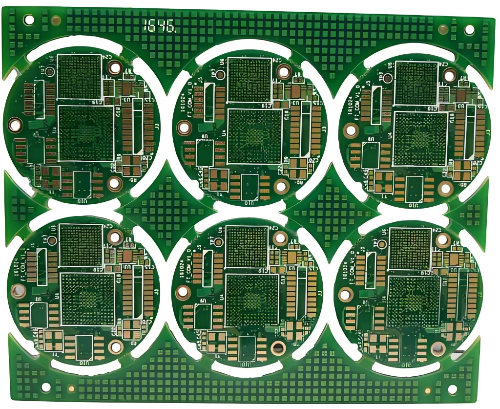
The most obvious issue in producing circular PCBs is the relatively high rate of raw material waste. Most PCB raw materials (such as FR4, CEM-1, and polyimide) are supplied as large rectangular sheets. When these are processed into circular structures, the central circular area is utilized, while the corners become scrap, making them difficult to reuse.
To improve raw material utilization, manufacturers typically employ the following strategies:
Panel design: Multiple circular PCBs are assembled into a single rectangular sheet to maximize layout efficiency. Common methods include “plum blossom” or “stepped” panels;
Optimized edge processing using laser cutting or V-cut methods: Precisely control the cutting line to reduce material waste;
Scrap recycling mechanisms: Establish a scrap sorting and reuse process to reduce production costs and environmental impact.
Machining precision control
During the processing of circular PCBs, the equipment required for operations such as drilling, contour milling, and slotting is more precise. The contours must be smooth and burr-free, especially for products used in rotating components or optical sensing, where high demands are placed on surface consistency.
CNC Milling Machine (CNC) Calibration: Using high-precision CNC equipment to cut circular shapes requires proper path radius and tool radius compensation settings.
Edge Grinding and Cleaning: Improve the smoothness of circular edges to prevent burrs that may affect installation or functional connection.
High Positioning Hole Accuracy Requirements: For circular boards with rotating or mating structures, the positioning holes must be symmetrically positioned with respect to the overall geometric center. Failure to do so may cause functional offset or weight imbalance.
Difficulty in Solder Mask, Character, and Silkscreen Alignment: Due to the unique shape of circular boards, standard printers may experience alignment errors during the silkscreen printing process, especially in high-volume production.
Customized Jig Design: Develop specialized jigs for positioning and securing circular boards.
Many Character Area Restrictions: The circular contour can create irregular character spacing, which can lead to layout constraints problem;
Local alignment adjustment mechanism: Some automated production lines support dynamic alignment correction using image recognition, making them suitable for fine-grained processing.
Electroplating and surface treatment uniformity
During the surface treatment process for round PCBs, current distribution uniformity must be considered. Common processes such as immersion gold (Immersion Gold), tinning, and OSP can all cause uneven treatment due to irregular edge shapes.
Electroplating rack design: Racks specifically designed for round PCBs should be designed to ensure uniform electrical potential across the entire board.
Adding copper rings or auxiliary structures to the outer frame: This ensures more balanced current distribution, preventing overplating in the center or underplating at the edges.
Processing fluid flow simulation: Based on multiple production experiences, equipment parameters are adjusted to ensure a more stable chemical treatment process.
Placement and back-end assembly adaptation: During SMT placement and back-end assembly, the shape of round PCBs dictates adjustments to the loading method, transport structure, and inspection process.
Non-standard carrier transfer: Custom jigs or the use of suction cup robots are required to transfer circular boards.
Increased optical positioning challenges: Especially in multi-function placement machines, additional visual calibration points are required.
Soldering support challenges: The lack of right-angle support surfaces makes warping and misalignment more likely during hot air soldering.
In summary, the manufacturing of circular PCBs goes beyond simply drawing a “circle” at the design level; it places higher demands on the entire processing chain. From material placement to precision control, surface treatment to assembly and adaptation, every step requires the support of an experienced engineering team and specialized equipment. These challenges are not insurmountable, but they must be factored into project planning from the outset and closely coordinated with production to ensure final delivery quality and cost efficiency.
Future Development Trends of Circular PCBs
With the continued emergence of wearable devices, medical electronics, smart home devices, and new energy products, circular PCBs are gradually evolving from niche applications to mainstream design. The following are possible development directions for this type of PCB in the coming years:
Evolution to Higher Density and Miniaturization
Since space constraints are a common challenge for circular PCBs, designers are continuously pushing for higher wiring density, smaller board thicknesses, and more compact structures. High-density interconnect (HDI) technology, multi-layer structures, and even buried and blind via solutions will become important means to enhance the performance of circular PCBs.
Integration with Flexible and Rigid-Flexible PCBs
To meet the needs of more diverse and three-dimensional design requirements, circular PCBs are increasingly being combined with FPCs (flexible printed circuits) or rigid-flexible PCBs. This is particularly true in products such as smartwatches and camera modules, where circular rigid PCBs are paired with peripheral flexible connectors, significantly improving space utilization and product aesthetics.
Enhanced Automated Cutting and Precision Forming Capabilities
Traditional circular PCB formation relies on CNC drilling and milling or laser cutting, which presents efficiency and cost challenges. In the future, improving the precision and speed of automated laser cutting, or adopting new processes such as die stamping, will significantly reduce circular PCB processing costs and increase production capacity.
Green and Environmentally Friendly Materials and Low-Carbon Processes
The global manufacturing industry is accelerating its transition toward green and sustainable development. In terms of material selection, circular PCBs will increasingly prioritize the use of environmentally friendly materials such as lead-free solder, halogen-free substrates, and recyclable copper-clad laminates. Furthermore, more energy-efficient and emission-reducing processes, such as water-saving etching and low-power exposure systems, will be incorporated into the production process.
Expanding Application Scenarios
As circular PCB technology matures, its applications are no longer limited to traditional handheld devices. In the future, we will see more circular PCBs in the following areas:
Medical sensors (such as skin-mounted heart rate monitors);
Automotive HUDs or in-vehicle display modules;
Wearable health devices, such as smart glasses and sleep monitoring rings;
Circular buttons and dial control circuits in human-computer interaction devices
Conclusion
Round PCBs, with their compact structure, flexible adaptability, and aesthetically pleasing design, are gaining an increasingly important position in modern electronic product design. From industrial intelligence to consumer electronics, from medical equipment to automotive electronics, circular PCB is not only a board type, but also a solution that breaks with tradition and pursues ultimate space utilization.