Definition and Basic Characteristics
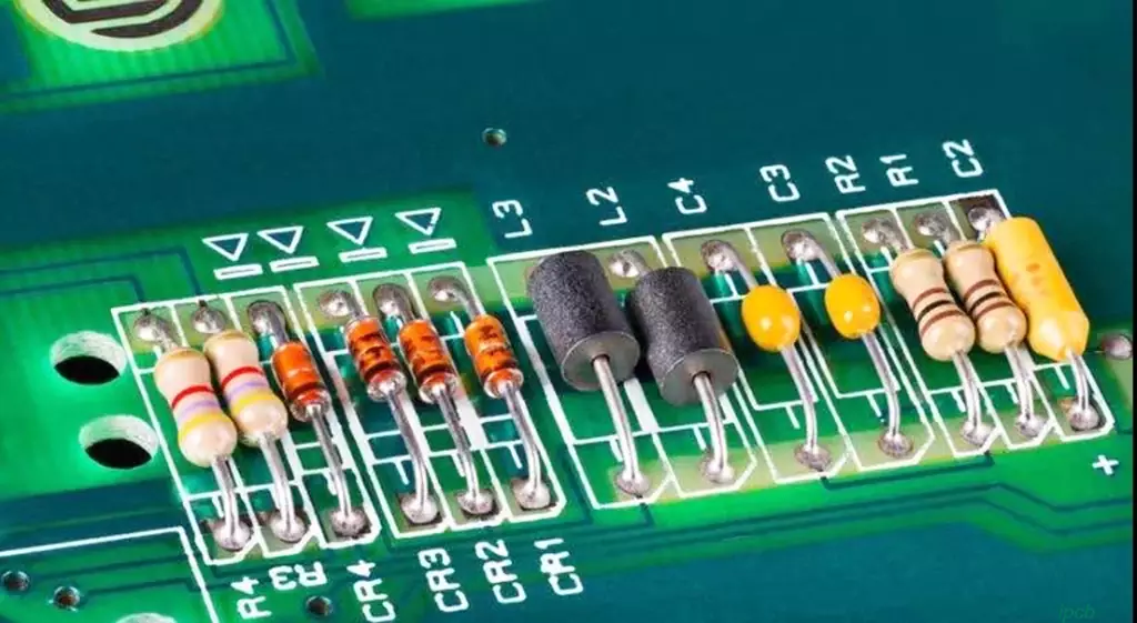
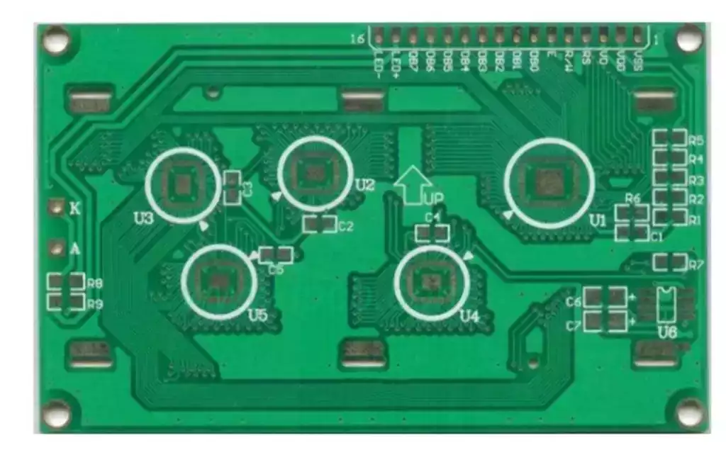
In the design and manufacturing of printed circuit boards (PCBs), exposed copper refers to surfaces with exposed copper, not covered by solder or solder mask. Exposed copper typically appears in areas requiring subsequent soldering, grounding, or testing, such as pads, vias, or conductive bridges. Compared to PCBs fully covered with solder mask, exposed copper areas offer direct conductivity, facilitating soldering, functional testing, and electrical connections for electronic components.
The characteristics of exposed copper PCBs are not limited to their physical structure but also dictate specific requirements for their manufacturing and use. First, because copper is highly susceptible to oxidation, exposed areas require strict protective measures during storage, transportation, and processing to prevent the formation of a copper oxide layer and ensure stable soldering and electrical performance. Second, because exposed copper areas are often exposed to the outside environment, higher requirements are placed on the PCB’s surface finish, cleanliness, and pad design accuracy.
In practical applications, exposed copper PCBs are commonly found in high-precision electronic devices, industrial control boards, and sensor modules. Its design principles emphasize both functionality and reliability: functionality ensures smooth electrical connections, while reliability guarantees long-term protection from contact problems or corrosion. The emergence of this type of board requires manufacturers to possess even stricter process control capabilities while meeting complex PCB requirements.
Beyond physical properties, the process used for bare copper PCBs directly impacts their performance. For example, whether electroless nickel/gold plating, tin spraying, or other protective treatments are used will affect soldering compatibility and longevity. Furthermore, the layout and size control of the bare copper areas are crucial for signal integrity and impedance matching, especially in high-speed, high-frequency, or high-density circuit designs.
In summary, exposed copper PCBs are not simply a variation of ordinary PCBs; rather, they represent a specialized board type that emphasizes the functionality, process control, and reliability of the bare copper areas. Their increasing application in modern electronics manufacturing provides a foundation for subsequent process optimization and high-performance product design.
Exposed Copper PCB Manufacturing Process and Precautions
The manufacturing process for exposed copper PCBs is more rigorous than that for conventional PCBs, as the bare copper areas have stringent requirements for oxidation, solderability, and surface finish. The entire process primarily includes substrate selection, pattern etching, surface treatment, and bare copper protection, each of which directly impacts the board’s electrical performance and reliability.
Substrate and Copper Foil Selection
The performance of bare copper PCBs begins with high-quality substrates and copper foil. Substrates typically use FR-4, high-Tg, or flexible materials to meet the heat resistance and mechanical strength requirements of different applications. The thickness of the copper foil is also crucial: too thin may cause melting during soldering or insufficient conductivity, while too thick may affect etching accuracy and line width control. For bare copper areas, it is recommended to use copper foil with high flatness, a thin oxide layer, and strong adhesion to ensure smooth subsequent processing.
Pattern Etching
During the etching process, line width, spacing, and bare copper area placement must be precisely controlled according to the design files. Bare copper areas require even higher etching precision, as any overetching or residual copper can affect soldering performance and impedance characteristics. Manufacturers typically employ high-precision photolithography and chemical etching processes, while also applying a protective film or mask to the bare copper areas to prevent corrosion during processing.
Surface Treatment
Bare copper areas are susceptible to oxidation, making surface treatment crucial. Common treatments include:
Electroless Nickel/Gold (ENIG): For bare copper areas requiring long-term protection or high-reliability soldering, a gold plating layer effectively prevents oxidation and improves solder wettability.
Halting/Hot Air Leveling (HASL): Suitable for bare copper areas with demanding soldering requirements, but temperature control is required to prevent substrate warping or trace damage.
Electroless Tin or Organic Protective Film (OSP): Suitable for short-term protection and low-cost PCBs, but with strict storage and operating requirements.
The choice of surface treatment requires a comprehensive consideration of the bare copper area’s service life, soldering method, and subsequent processing steps.
Bare Copper Area Protection and Quality Control
During manufacturing and storage, bare copper areas must be protected from air, moisture, or corrosive substances. Common protective measures include:
Local protective film covering, removed only before soldering; inert gas packaging to reduce oxidation risks; and strict environmental control, such as constant temperature and humidity workshops and dry packaging.
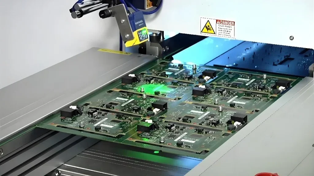
In addition, quality control of bare copper PCBs requires enhanced electrical testing and visual inspection. Any minor defects in the bare copper area can cause shorts, opens, or poor soldering. Therefore, manufacturers often perform additional AOI (automated optical inspection) or electrical testing on the bare copper area to ensure that the board meets design requirements before shipment.
Application Scenarios and Advantages of Exposed Copper PCBs
Application Scenarios
Exposed copper PCBs are widely used in electronic products requiring high-reliability connections, heat dissipation, or specific electrical functions. Typical applications include:
Consumer electronics. In smartphones, tablets, and wearable devices, exposed copper pads are critical areas for component mounting, ensuring secure soldering of chips, capacitors, inductors, and other devices. In flexible circuits, exposed copper areas are often used for contact with FPC connectors to enable fast transmission of high-frequency signals.
Automotive electronics. In automotive electronic control modules (ECUs), radar sensors, and battery management systems (BMS), bare copper PCBs carry higher current densities and complex control signals. Bare copper areas not only facilitate high-current soldering but also maintain good contact performance in harsh environments.
Industrial control and power supply equipment. Bare copper PCBs are widely used in industrial power supplies, motor drives, sensors, and PLC control units. Bare copper pads can withstand high currents and high-frequency switching, ensuring the stability of the equipment during continuous operation.
Medical electronics. Medical devices require extremely high signal integrity and reliability. Bare copper areas are often used for sensor interfaces and electrode connections to ensure data transmission is immune to external interference while maintaining low contact resistance and high sensitivity.
Communications and high-speed circuits. In 5G communication base stations, network routers, and high-speed computing equipment, bare copper PCBs facilitate high-speed interconnects and low-loss signal transmission, meeting the requirements for high-frequency signal integrity and impedance control.
Advantage Analysis
Compared to PCBs fully covered with solder mask, exposed copper PCBs offer the following significant advantages:
Strong soldering reliability. Bare copper pads provide a direct soldering interface for component mounting, ensuring strong solder joints and higher soldering efficiency while reducing the risk of cold joints and desoldering.
Excellent electrical performance. Bare copper areas ensure low contact resistance and high conductivity, making them particularly suitable for high-frequency signal transmission and high-current carrying, ensuring stable circuit performance.
Excellent heat dissipation. Copper has excellent thermal conductivity, and bare copper areas serve as heat dissipation channels, quickly transferring heat to a larger copper foil or heat sink structure, improving the overall heat dissipation capacity of the PCB.
High process flexibility. Depending on the application requirements, bare copper areas can be plated with gold, sprayed with tin, or left raw to achieve a different balance between cost control and performance.
Easy to test and repair. Bare copper pads or test points facilitate subsequent electrical testing and repair, making quality control and rework more efficient.
Challenges and Limitations
While their advantages are clear, bare copper PCBs also present certain challenges:
They are susceptible to oxidation, requiring strict protection during storage and transportation; surface treatment processes are costly; and high-precision etching of bare copper areas requires manufacturers to possess advanced process capabilities.
Therefore, bare copper PCBs are often used in applications that require high performance and high reliability, not all low-end electronic products require this process.
Key Design Points and Engineering Considerations for Exposed Copper PCBs
Designing exposed copper PCBs is not as simple as randomly adding a few exposed copper pads in a circuit diagram. It is a systematic project that balances electrical performance, process feasibility, and long-term reliability. The following aspects are key considerations during the design phase:
Layout Planning of Exposed Copper Areas
Exposed copper areas are typically used for component soldering points, heat sinks, or test points. Their layout directly impacts circuit functionality and assembly efficiency.
Pad Layout: Ensure that the dimensions match the component pins, ensuring secure soldering while avoiding excessive or insufficient solder.
Heat sinks: Design a larger exposed copper area beneath high-power devices to facilitate heat dissipation. However, thermal vias should be incorporated to prevent localized heat buildup.
Test point layout: Standardized and standardized, ensuring easy probe access and compatibility with automated test equipment.
Designing the Clearance Between Solder Mask and Bare Copper
The accuracy of the solder mask opening directly determines the quality of the bare copper area. Excessive openings can cause the bare copper to grow outward, increasing the risk of oxidation; too small openings can compromise soldering reliability. Designs typically require a reasonable clearance between the solder mask and bare copper (typically 3–5 mils) to ensure full exposure of the pads while minimizing damage to surrounding traces.
Matching Surface Finishes
Different application scenarios require different surface finishes for bare copper areas:
ENIG (nickel-gold plating) is recommended for high-end communications or medical electronics, ensuring long-term reliability and excellent soldering performance.
Anti-spray tinning (HASL) is an option for high-volume consumer electronics, maintaining cost control while maintaining good soldering compatibility.
Organic overprint stencil (OSP) can be used for short-term or cost-sensitive products, but be aware of shelf life limitations.
Designers must discuss the feasibility of surface finishes with manufacturers early on; otherwise, yield reduction and cost overruns may occur during mass production.
Design Considerations for High-Frequency and High-Speed Signals
In high-speed circuits, the size and shape of the bare copper area can affect impedance and signal integrity. For example, oversized exposed copper pads can introduce parasitic capacitance, causing high-speed signal reflections or delays. Therefore, when designing exposed copper areas, simulation tools should be used to assess their impact on electrical performance. Risks can be mitigated by optimizing the layout or adding ground vias.
Environmental and Reliability Requirements
For PCBs operating in complex environments (such as automotive electronics or industrial control equipment), designers must consider the reliability of exposed copper areas in high temperatures, high humidity, or corrosive atmospheres. If necessary, additional protection should be implemented, such as adding protective shields to the exposed copper areas or adding redundant solder joints to the system design to prevent single points of failure.
Manufacturing and Assembly Compatibility
The design of bare copper PCBs must also consider compatibility with surface-mount (SMT), wave soldering, or manual soldering processes. For example, undersized exposed copper pads can cause solder misalignment during automated placement, while oversized pads can easily cause solder bridging. Only by fully considering assembly processes during the design phase can rework and scrap be avoided during subsequent mass production.
Inspection and Quality Control of Exposed Copper PCBs
Exposed copper PCBs are unique in that portions of the copper foil are exposed, serving as both electrical connections and soldering or heat dissipation interfaces. This makes them more susceptible to environmental influences during production and storage, making inspection and quality control particularly critical.
Appearance Inspection: Appearance inspection is the first line of defense before PCBs leave the factory. Bare copper areas require special inspection for the following issues:
Oxidation and Discoloration: Bare copper easily oxidizes when exposed to air, forming dark spots or discoloration, which directly affects soldering performance.
Scratches and Depressions: Scratches caused by mechanical handling or production can damage the integrity of the copper surface and even affect electrical conductivity.
Solder Mask Shift: Misalignment of the solder mask openings can result in insufficient or excessive exposed copper area.
A combination of manual microscopy inspection and automated optical inspection (AOI) is typically used to ensure timely detection of defects.
Electrical Performance Testing
Because bare copper pads are often used for soldering and electrical interconnection, their electrical conductivity must be guaranteed. Inspection steps include:
Continuity testing: Verifying that the bare copper area is properly connected to the circuit;
Insulation testing: Ensuring that there are no shorts between the bare copper and surrounding traces or pads;
Contact resistance testing: Assessing whether the bare copper surface’s conductivity remains within acceptable limits.
These tests are typically performed using a flying probe tester or a dedicated fixture tester to ensure the electrical reliability of each circuit board.
Surface Finish Quality Verification
Bare copper PCBs often undergo surface treatment before shipment, so the integrity of the treatment layer must be verified:
Gold plating thickness and uniformity inspection: For ENIG processes, the gold layer thickness must be uniform and meet IPC standards;
Holing process uniformity inspection: Ensure complete tin coverage to avoid oxidation risks caused by too thin a layer or soldering difficulties caused by too thick a layer;
OSP coverage verification: While difficult to detect with the naked eye, chemical testing or microscopic observation can confirm effective coverage of the copper surface.
Environmental Stress Testing
To ensure the long-term reliability of bare copper areas, manufacturers typically conduct a series of environmental stress tests:
High-Temperature and High-Humidity Testing: Verifies whether bare copper corrodes in humid environments;
Hot and Cold Shock Testing: Simulates the temperature cycles experienced by the PCB in its operating environment to detect cracking or failure of solder pads;
Salt Spray Testing: Verifies the corrosion resistance of bare copper surfaces, particularly for automotive electronics or marine applications.
These tests are critical steps in evaluating the long-term reliability of PCBs.
Quality Control Process
To ensure the consistency and reliability of bare copper PCBs, companies need to establish a comprehensive quality management system:
Incoming Material Inspection: Checks the quality of copper foil and solder mask ink;
Process Monitoring: Establishes quality control points in key processes such as etching, solder mask opening, and surface treatment;
Factory Inspection: Conducts full or random inspections in strict accordance with IPC standards to ensure that each PCB meets customer requirements;
Traceability: Uses barcodes or QR codes to trace production batches and test results, facilitating after-sales problem analysis and improvement.
Future Development and Industry Trends of Exposed Copper PCBs
As the demand for performance, reliability, and miniaturization in electronic products continues to increase, the application scope of exposed copper PCBs will continue to expand, and their design and manufacturing processes will inevitably evolve accordingly. Future development trends can be observed from the following aspects:
High-density interconnection and miniaturization trends
Modern electronic devices, especially smart wearables, medical implants, and 5G communication modules, require PCBs to be smaller and more complex. Exposed copper areas, as critical soldering and connection interfaces, will continue to evolve towards smaller sizes and higher precision. This means that the precision requirements for solder mask openings and surface treatment will be even higher, posing a severe challenge to manufacturers’ process capabilities.
More Environmentally Friendly Surface Treatment Technologies
Currently Common Surface Treatment Methods for Bare Copper PCBs All electroplating processes (such as tin spraying, ENIG, and OSP) have certain environmental restrictions. For example, some electroplating processes involve heavy metals, potentially impacting the environment. As environmental regulations become increasingly stringent, more new lead-free, low-pollution, and recyclable surface treatment materials and processes will emerge to meet the green manufacturing requirements of the global market.
Optimization for High-Speed and High-Frequency Applications
In high-speed signal transmission and high-frequency circuits, the shape and distribution of bare copper areas directly impact signal integrity. With the development of emerging fields such as 5G, AI servers, and autonomous driving, bare copper PCBs will place greater emphasis on impedance control, parasitic reduction, and electrical performance optimization. This requires not only more intelligent design software but also manufacturers to provide more precise process coordination.
Integration with Flexible Circuits and Multilayer Stacking
In the future, PCBs will move beyond single rigid boards and increasingly utilize rigid-flex PCBs or high-layer stacking. This trend will expand the application of bare copper areas. For example, bare copper pads in flexible circuits require greater mechanical strength and flex resistance. This will drive further innovation in related materials and processes.
Intelligent Inspection and Quality Control
With the development of Industry 4.0 and smart manufacturing, traditional inspection methods that rely on manual labor or single methods will gradually be replaced by inspection systems driven by big data and AI. In the future, bare copper PCB inspection will no longer simply determine whether a product is acceptable or not. Instead, data accumulation and analysis will be used to predict defects, optimize processes, and even provide early warnings during the design phase. This predictive quality management will significantly improve yield and reliability.
Further Expansion of Applications
Beyond consumer electronics and communications, demand for bare copper PCBs will continue to grow in new energy (such as power battery management systems), medical electronics (high-reliability sensor interfaces), and automotive electronics (power device heat dissipation and interconnects). In particular, the heat dissipation advantages of bare copper areas will gain wider application and recognition in high-power and high-heat dissipation scenarios.
Summary
Exposed copper PCBs, a seemingly common yet crucial design and process in electronics manufacturing, play an irreplaceable role in soldering performance, heat dissipation capacity, and electrical connection reliability. From manufacturing processes and surface treatment to quality inspection, every step directly determines their long-term stability and application value. As the electronics industry continues to move toward higher density, miniaturization, and higher performance, bare copper PCBs must not only meet current process requirements but also adapt to future developments through innovations in environmentally friendly materials, intelligent testing, and cross-domain applications.
A bare copper PCB is more than just the “exposed copper surface” of a circuit board; it represents a comprehensive reflection of connection reliability and manufacturing technology. Understanding and mastering its design and process not only helps companies enhance their competitiveness but also provides a solid foundation for the advancement of the entire electronics industry.