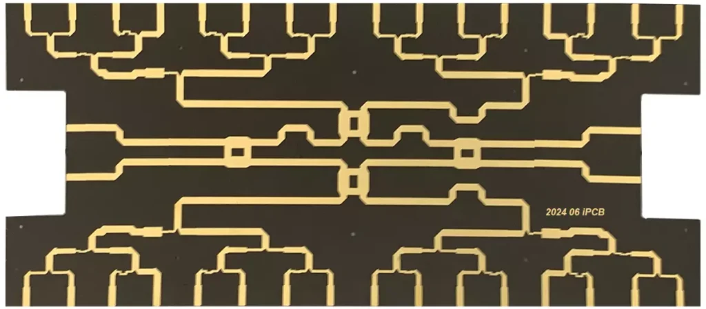
What is antenna PCB? Antenna PCB is a wireless communication component based on printed circuit boards, widely used in the field of wireless communication. Antenna PCBs are an indispensable part of modern electronic devices, especially playing a crucial role in wireless communication. It is a special type of printed circuit board that integrates antenna function. This type of PCB uses printing technology to print wires on insulating materials, forming an antenna structure for receiving and transmitting wireless signals.
Antennas are an important component of wireless communication systems, typically containing one or more PCBs that carry important signal processing and analysis functions of the antenna. The antenna PCB is used for transmitting and receiving wireless signals. It achieves wireless communication by converting electromagnetic energy into wireless signals or converting wireless signals into electromagnetic energy. The working principle of the antenna is based on the principles of electromagnetic radiation and reception, using the electromagnetic field generated by the current in the conductor to achieve signal transmission.
Antenna PCBs usually use high-frequency PCB materials, such as Rogers PCB, RO4350B PCB, RO4003C PCB, RT5880 PCB, RO3003 PCB, Taconic PCB, PTFE PCB, Teflon PCB, etc
The antenna circuit board not only transmits signals, but also carries important functions of processing and analyzing signals.
- Filter noise: The antenna circuit board can improve the signal quality received by the antenna by filtering out external interference signals.
- Amplify signal: The crystals and amplifiers in the antenna circuit board can amplify the signal received by the antenna, thereby improving the sensitivity of the receiver.
- Signal processing: The circuits and processors in the antenna circuit board can process and analyze the signals received by the antenna, thereby improving its recognition and positioning performance.
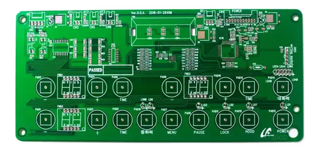
What are the requirements for antenna PCB design? The accuracy of antenna PCB positioning, substrate manufacturing program, substrate size, and probe type are all factors that affect detection reliability.
- Accurate positioning holes: Set precise positioning holes on the substrate, with an error of ± 0.05mm. At least two positioning holes should be set, and the farther the distance, the better. Using non-metallic positioning holes to reduce the thickening of the solder coating without meeting the tolerance requirements. If the substrate is manufactured as a whole and then tested separately, the positioning holes must be located on the main board and each individual substrate.
- The diameter of the test points should not be less than 0.4mm, and the distance between adjacent test points should be at least 2.54mm, not less than 1.27mm.
- High components should not be placed on the testing surface as they may cause poor contact between the online testing fixture probe and the testing point.
- It is best to place the test points 1.0mm away from the vicinity of the components to avoid impact damage between the probe and the components. Within 3.2mm around the positioning hole ring, there should be no components or test points.
- The testing point cannot be set within a range of 5mm from the edge of the PCB, and this 5mm space is used to ensure the clamping of the fixture. Usually, the same process edge is required in conveyor belt production equipment and SMT equipment.
- All detection points should be tinned or selected with soft, easily penetrating, and non oxidizing metal conductors to ensure reliable contact and extend the service life of the probe.
- The test point should not be covered with solder mask or text ink, otherwise it will reduce the contact area of the test point and reduce the reliability of the test.
The design of antenna PCB board includes key points such as antenna size, layout, and matching.
- Antenna size: The selection of antenna pcb size is related to the operating frequency and antenna radiation characteristics. The larger the size, the better the radiation effect, but at the same time, it will lead to an increase in PCB board size, cost, and manufacturing difficulty.
- Antenna layout: Optimization of antenna layout can improve the radiation efficiency and directionality of the antenna. A reasonable layout can reduce mutual interference and impedance matching issues between antennas.
- Matching: The matching between the antenna and the feeder is the key to ensuring the normal operation of the antenna. Poor matching can lead to increased signal transmission loss and decreased radiation efficiency.
The antenna PCB is an indispensable component of the antenna. It carries important functions of antenna signal processing and analysis, improving the receiving performance and positioning accuracy of the antenna through filtering noise, amplifying signals, and processing signals.
The working principle of the high-frequency antenna circuit board determines the performance and reliability of the antenna. Reasonable design and optimization can improve the radiation efficiency, directionality, and anti-interference ability of antennas. With the increasing development of wireless communication and radar technology, the requirements for high-frequency antenna PCB boards are also increasing, such as wider operating frequency bands, higher radiation efficiency, and smaller size. With the continuous development of wireless communication and radar technology, the working principle of antenna PCB will continue to be deeply studied and developed.
iPCB is an antenna PCB circuit board manufacturer that regularly stocks various high-frequency PCB materials and provides fast prototyping and mass production services, such as microwave antenna PCB, high-frequency antenna PCB, high-frequency PCB board, RF PCB board, and Hybrid high-frequency circuit boards.