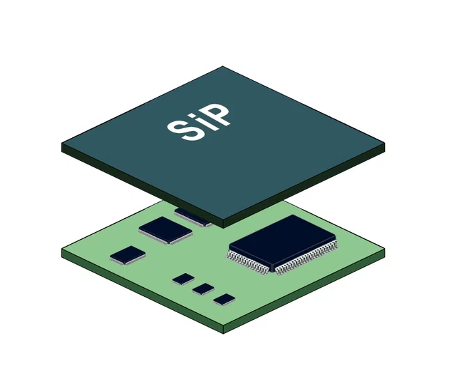
System in Package (SIP) is a packaging method that integrates multiple semiconductor chips and passive components vertically or horizontally in a single package module. Compared with traditional multi-chip packaging (MCM), SIP package emphasizes functional unitization and module integration, which can improve design flexibility and integration.
SIP packaging has the following important technical features:
Chip vertical/horizontal stacking: realize device integration of different functions (such as logic, storage, and radio frequency)
High-density interconnection: use micro-bumps, ultra-fine lines or ABF substrate technology to maintain high-speed signal integrity
Functional composite packaging: integrate multiple functional modules such as sensors, power managers, and microcontrollers
SIP packaging can be divided into the following main structures:
Stacked stack structure
Use adhesive or bumps for interlayer connection to stack multiple chips vertically, such as logic + memory chips in a single package;
Horizontal side-by-side structure
Place multiple devices on the same substrate and interconnect them through high-density wiring, which is suitable for multi-functional side modules;
Mixed stacking structure
Use vertical stacking and side-by-side layout at the same time to meet the needs of higher integration;
Three-dimensional interconnection structure
Use through silicon via (TSV), flip chip, and silicon interposer technology to achieve 3D-level compact integration.
Differences from SiP, MCP, and SoC
SoC (System on Chip) integrates all functions into a single chip, which is complex in design but high in cost and power consumption;
MCP (Multi-Chip Package) is similar to inserting multiple independent chips without system-level design;
SiP/SIP is between the two, with advantages in modular integration and design reusability
Manufacturing process of SIP packaging
The manufacturing process of System in Package is relatively complex and requires the cooperation of multiple high-precision processes. A complete SIP packaging manufacturing process usually includes the following core steps:
Chip preparation and testing
Before packaging begins, all chips used for SIP need to undergo wafer-level electrical testing (Wafer Test) to screen out chips with qualified performance and separate them into separate Dies through a cutting process.
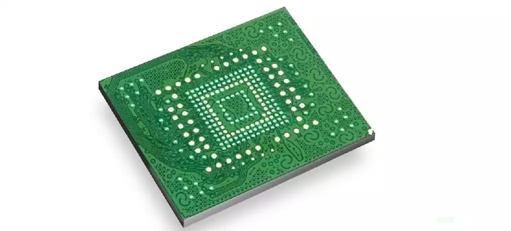
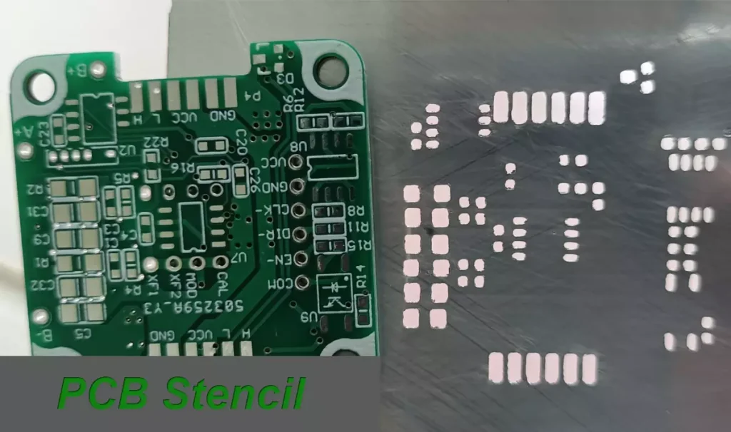
Substrate design and manufacturing
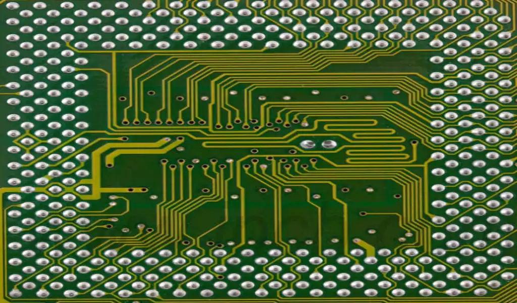
The packaging substrate used by SIP is different from traditional PCBs. It generally uses high-density interconnect (HDI) or Ajinomoto Build-up Film (ABF) substrate technology. This type of substrate must have high-frequency signal support, fine line width/pitch control, and multi-layer stacking capabilities.
Chip Interconnection
The main interconnection methods are as follows:
Flip Chip: reversely mounted on the substrate through solder balls;
Wire Bonding: suitable for structures with sufficient space and simple functions;
TSV (Through Silicon Via): used for vertical connections in high-end 3D packaging, with high efficiency but high manufacturing cost.
Multi-chip packaging stacking
The chips are stacked through interposers or directly stacked to achieve three-dimensional space utilization. Precise alignment is required during the packaging process to ensure a good interconnection path.
Packaging and Molding
The chip stacking structure is protected by epoxy resin molding, plastic sealing or metal cover sealing. Some high-end products use liquid packaging materials to improve thermal conductivity.
Packaging Testing and Sorting
After the packaging is completed, the final electrical test (Final Test), aging test and functional verification are required to ensure that all systems work well together in the package to avoid the phenomenon of “good core and bad seal”.
Key Technologies and Challenges
Although SIP brings the advantages of high integration and functional combination, it also faces many technical challenges in its design and manufacturing process.
Thermal management issues
Multi-chip packaging often leads to local heat accumulation and complex heat dissipation paths. Thermal design in SIP requires the use of thermal conductive fillers, metal heat sinks, thermal vias, etc. to avoid overheating damage.
Electrical performance integrity
The interconnection between high-frequency chips must consider signal integrity issues. The transmission line structure, impedance matching and stratum distribution must be optimized in the design stage to reduce crosstalk and noise.
Package stress and reliability
Multi-layer chip stacking is prone to inconsistent thermal expansion, resulting in cracking of the internal structure due to thermal stress. Therefore, it is necessary to introduce low CTE materials and structural design optimization, such as buffer layers and flexible substrates.
Material compatibility issues
There are differences in expansion coefficient, hardness, electrical properties, etc. between different chip sources and different packaging materials. If they are not matched properly, the reliability and life of the package will be seriously affected.
Typical application areas
SIP packaging plays a key role in many fields due to its miniaturization, high integration, modularization and other characteristics.
Smartphones and wearable devices
The RF front-end modules (RFFE) commonly used in mobile phones are mostly SIP packages, integrating PA, LNA, Switch and other modules to improve communication stability; smart watches often integrate MCU, MEMS, Bluetooth and other devices in SIP.
IoT IoT terminals
Many IoT nodes need to integrate sensors, MCU, communication modules and power management chips. SIP packages provide compact solutions suitable for space-constrained environments, such as smart homes and industrial remote monitoring.
Automotive electronic systems
ADAS, radar modules, battery management and other functions are increasingly SIP-based, promoting the miniaturization and high reliability of electronic control units and improving the intelligence level of the entire vehicle.
Medical devices and implantable electronics
SIP packaging makes portable, wearable and even implantable medical devices possible, especially in high-demand fields such as ECG sensors and neurostimulators.
Signal interference and electromagnetic compatibility (EMC) issues
As more and more chips are integrated into SIP packages, especially when RF modules, storage, MCUs and even power management chips are included, electromagnetic interference (EMI) issues between different functional units have become increasingly prominent. The frequency span of the signal inside the system is large and the wiring space is limited. If not properly handled, it is very easy to cause signal integrity problems such as crosstalk, radiation interference, and common mode noise.
To this end, a variety of EMC control measures need to be adopted in SIP design:
Optimize the wiring structure: By reasonably dividing the ground layer and the power layer, using differential routing, return path control and other methods to reduce the radiation path;
Introduce shielding technology: Add an EMI shielding layer or use EMC resin coating inside the package to physically isolate the high-frequency source;
Package layout planning: Separate high-noise modules (such as RF chips, DC-DC modules) from sensitive modules (such as analog sensors) and use signal absorption structures;
Material selection optimization: Use dielectric materials with good high-frequency performance, such as low Dk and low Df substrates, to reduce signal loss and crosstalk.
In addition, the SIP as a whole needs to pass strict EMC testing and certification, such as radiation emission and anti-interference tests under IEC and CISPR standards, to ensure that it can operate stably in complex systems.
Detection, verification and quality control
SIP technology is complex, and any small process deviation may cause system failure. Therefore, its detection and quality control are particularly critical.
X-ray and CT analysis
Perform nondestructive testing of chip interlayer connections to evaluate defects such as solder joint integrity, offset, and voids.
Electrical function test
Includes DC/AC parameter test, logic function verification, dynamic response, etc. to ensure communication coordination between chips.
Thermal cycle test
Evaluate the thermal stability and welding reliability of the SIP structure through high and low temperature alternating tests.
Highly accelerated life test (HAST)
Simulates humid, high temperature, and high pressure environments to test device durability and package sealing performance.
Future development trends and technological innovation
SIP technology is still evolving, and its future development shows the following major trends:
Heterogeneous integration is the general trend
Integrate and package chips of different process nodes (such as 5nm logic + 28nm storage) to maximize performance and cost advantages, and promote the application of high-performance computing and AI chips.
Development of advanced packaging substrates
New packaging substrates such as ABF, Fan-Out, and RDL will further support high-density wiring and smaller spacing, breaking through the physical limitations of traditional HDI boards.
Automation and AI design are accelerating their popularity
EDA tools and AI-assisted design software will improve the efficiency of SIP system-level design, realize functional modularization, simulation automation and intelligent packaging integration.
SIP + Chiplet Fusion
Chiplet design ideas are combined with SIP packaging, using interposers or 2.5D packaging methods to assemble modules from different manufacturers, promoting packaging standardization and ecological co-construction.
Summary
As an important branch of modern packaging technology, System in Package is driving electronic products from decentralized integration to compact, modular, and high-performance. It achieves more functional combinations with a smaller volume, providing great freedom for chip-level system development. From smartphones, IoT terminals to high-performance automotive electronics and wearable medical devices, SIP is silently changing the entire electronic manufacturing landscape.
Of course, SIP’s path forward is not without challenges. How to deal with signal interference between chips, how to achieve efficient heat dissipation in a limited space, and how to be compatible with different types of chip structures and process platforms, these technical barriers still need to be continuously broken through. Fortunately, with the intelligence of EDA tools, the continuous innovation of packaging substrates, and the diversification of material systems, these problems are gradually being overcome.
In the future, SIP will intersect with trends such as Chiplet, 2.5D/3D packaging, and advanced interposer technology to build a more flexible, powerful, and configurable system architecture. It can not only adapt to the commercial needs of rapid product iteration, but also show great potential in cutting-edge fields such as artificial intelligence, 5G, in-vehicle computing, and high-end medical care.
For enterprises, whoever can take the lead in the SIP packaging field, quickly mass produce, and optimize costs will gain an advantage in the fierce competition. For technicians and newcomers in the industry, mastering the basic concepts, design principles, and process flow of SIP is undoubtedly the “ticket” to enter the world of high-end packaging.
SIP is not the end, but the starting point of the next round of technology competition.