The concept and importance of Board PCB Assembly
In modern electronics manufacturing, board PCB assembly is a core link connecting design concepts and finished product functionality. It’s not merely about soldering electronic components onto circuit boards; it’s a crucial guarantee for the stable operation, reliability, and high performance of the entire electronic product. As electronic products evolve towards miniaturization, high density, and multifunctionality, the PCB assembly process demands higher standards in precision, reliability, process control, and material selection. Even a well-designed PCB can be negatively impacted by soldering deviations, component misalignment, solder joint defects, or temperature damage during assembly, directly affecting the performance and lifespan of the final product and potentially even posing safety hazards.
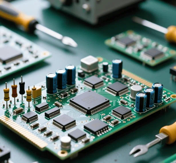
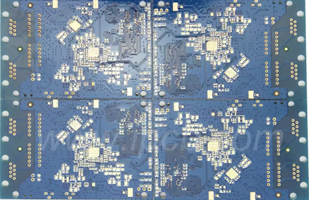
From a process perspective, board PCB assembly involves multiple steps, including surface mount technology (SMT), through-hole technology (THT), wave soldering, reflow soldering, manual soldering, and final inspection and testing. Each step requires strict process control and sophisticated equipment. For example, SMT is a core method for modern high-density PCB assembly, enabling the precise mounting of tiny packaged electronic components onto the PCB while ensuring the reliability of the solder joints. Through-hole (PTH) technology is primarily used for components requiring through-holes, achieving stable mechanical fixation and electrical connection through PTH holes. Wave soldering and reflow soldering processes ensure reliable conductivity and mechanical strength at all solder joints. Deviations in any step can lead to poor PCB assembly, affecting overall system performance.
PCB assembly also plays a crucial role in cost control and product yield. Efficient assembly processes not only shorten production cycles and reduce labor costs but also significantly improve first-pass yield. Conversely, non-standard assembly processes, inaccurate soldering temperature control, and inadequate component arrangement and storage management can lead to increased rework rates, material waste, and delivery delays. This is especially important for large-scale production, as the efficiency and stability of the assembly process directly impact a company’s profit margins and market competitiveness.
Furthermore, with the diversification of electronic product functions and increasing technological complexity, PCB assembly is no longer just a matter of mechanization; it demands systematic quality control and intelligent management. Modern factories typically utilize automated placement machines, intelligent visual inspection systems (AOI), X-ray inspection (AXI), and in-circuit testing equipment to monitor every step of the PCB assembly process in real time. This high-precision, highly automated assembly model transforms board PCB assembly from a simple soldering operation into a core technological link ensuring the stability, reliability, and high performance of electronic products.
In short, board PCB assembly is the bridge connecting design concepts and product performance; it is a crucial link in the transformation of electronic products from schematics to physical devices, and from functional implementation to stable and reliable operation. It requires not only engineers with solid circuit knowledge and assembly process understanding but also manufacturing teams with high levels of expertise in equipment management, process flow, and quality control. Mastering this technology is invaluable for companies in enhancing product competitiveness, reducing production risks, and ensuring customer satisfaction.
Board PCB Assembly Process Flow and Key Control Points
The core objective of board PCB assembly is to transform the circuit design on the PCB into a fully functional and stable electronic product. Achieving this goal requires a series of precise and complex processes, each of which must be strictly controlled to ensure the reliability and functionality of the final product. Modern PCB assembly typically includes steps such as surface mount technology (SMT), through-hole mounting (THT), soldering, cleaning, inspection, and final testing. Each step involves material selection, temperature management, mechanical precision, chemical processes, and quality control.
First is the surface mount technology (SMT) process, the core of high-density PCB assembly. SMT requires pick-and-place machines to accurately place components onto the PCB pads with micron-level precision. Deviations in placement can lead to short circuits, cold solder joints, or component misalignment, thus affecting the stability of the entire circuit. To ensure placement accuracy, manufacturing plants typically equip themselves with high-precision pick-and-place machines and automated feeding systems, combined with solder paste printing processes to precisely control solder paste thickness and distribution, ensuring soldering quality. Furthermore, component storage and moisture protection are crucial for SMT success; excessive humidity or improper handling of electrostatic-sensitive components can cause solder joint defects or component damage during reflow soldering.
Next is the through-hole mounting (THT) process, primarily used for mounting through-hole components. THT (Through-Hole Tolerancing) components not only provide electrical conductivity but also play a role in mechanical fixation, such as securing large capacitors, inductors, or connectors. The through-hole process involves component insertion, soldering, and wave soldering or manual soldering. Each step requires that hole diameter tolerances, pad sizes, and solder flow meet standards. For complex multilayer PCBs, the insertion sequence and thermal management of THT components are particularly critical. An improper sequence or unstable soldering temperature can lead to excessive localized thermal stress, affecting other components or circuits.
Soldering is one of the most crucial aspects of PCB assembly, including reflow soldering and wave soldering. Reflow soldering is primarily for SMT components, controlling the solder paste melting temperature profile to ensure uniform soldering of component leads. Excessive soldering temperature can damage components or the PCB substrate, while insufficient temperature can result in cold solder joints or bridging. Wave soldering is used for THT components and double-sided boards, requiring control of solder wave height, speed, and temperature profile to ensure reliable soldering of each lead without solder balls or short circuits. During the soldering process, manufacturers also need to pay attention to the solder composition, PCB surface treatments (such as HASL, ENIG), and soldering sequence, as these factors all affect the long-term reliability of the solder joints.
After soldering, cleaning and surface treatment are equally important. Solder residue can absorb moisture in humid environments, reducing the PCB’s insulation performance or causing electrochemical corrosion. High-quality boards are typically treated with specialized cleaning solutions and undergo drying and baking processes to remove moisture and volatiles, ensuring a clean, residue-free PCB surface. Additionally, some special applications require the addition of protective coatings, such as solder mask or protective coatings, to improve the board’s moisture and corrosion resistance, extending product lifespan.
Finally, there is the inspection and testing stage, which is the last line of defense for ensuring PCB assembly quality. Modern factories use AOI (Automated Optical Inspection), X-ray inspection, ICT (In-Circuit Testing), and functional testing to perform multi-level inspections on each PCB. AOI (Automated Optical Inspection) can detect component misalignment, polarity errors, missing components, or abnormal solder paste; X-rays can inspect hidden solder joints such as BGAs; ICT (Information and Technology Testing) can quickly detect electrical continuity, short circuits, or open circuits; functional testing simulates end-use scenarios to verify overall system performance. Data feedback from each stage is not only used for quality control but also provides a reference for subsequent process optimization, forming a closed-loop management system to ensure PCB assembly reliability meets design requirements.
Overall, board PCB assembly is not a single operation but a highly integrated system engineering project. Every step—whether it’s SMT (Surface Mount Technology), THT (Through Thorough Testing), soldering, cleaning, or inspection—must be meticulously managed in terms of materials, equipment, processes, and quality control. Only by fully understanding and optimizing these processes can high yield and sustainable production be achieved while ensuring product functionality, reliability, and production efficiency.
Board PCB Assembly Quality Control and Defect Management
Throughout the entire board PCB assembly process, quality control is integrated into every detail. It determines whether the product has stable electrical performance, sufficient mechanical strength, and long-term reliability. The ever-increasing demands of modern electronic devices for high density, high precision, and high stability mean that even minor defects in the PCB assembly process can be amplified into functional failures in the final product. Therefore, establishing a comprehensive quality management system, deeply understanding the formation mechanisms of various assembly defects, and implementing proactive prevention and timely correction within the process are crucial for improving production yield and product competitiveness.
First and foremost, the importance of soldering quality control must be emphasized. In SMT processes, solder paste printing is the fundamental step determining solder joint quality. Excessive solder paste can easily lead to solder joint bridging; insufficient solder paste can result in cold solder joints or weak solder joints. To ensure printing stability, the manufacturing end must control the stencil thickness, aperture shape, squeegee pressure, and printing speed. Simultaneously, the reflow soldering temperature profile is another critical factor determining solder joint reliability. An excessively short preheating zone may result in incomplete solvent evaporation and solder balls; insufficient reflow zone temperature can cause cold solder joints; and excessively rapid cooling can increase internal stress in the solder joint, affecting long-term reliability. Therefore, the reflow oven temperature profile typically needs to be precisely adjusted according to different component packages and PCB materials to ensure good wetting and solder joint formation.
Secondly, defect management in the THT process is equally critical. The soldering of through-hole components is affected by the thickness of the through-hole metallization, pad size, lead length, and solder flowability. During wave soldering, uneven temperature or improper flux distribution can easily lead to problems such as solder spikes, solder balls, cold solder joints, or bridging. Air bubbles or contaminants within the through-hole can also cause incomplete soldering. To avoid these common defects, factories typically implement strict controls on open-circuit current, solder wave height, transfer speed, and flux application. Furthermore, large through-hole components require special attention to mechanical stress caused by thermal expansion and contraction to prevent pad lifting or circuit delamination due to temperature shocks during soldering.
In the quality management system, the control of component quality and storage environment is also crucial. Moisture is one of the main risk factors leading to soldering failure, especially for components sensitive to IC, BGA, and QFN packages. If these components absorb moisture and are directly subjected to high-temperature reflow soldering, the internal moisture expansion can cause a “popcorn effect,” leading to damage to the internal structure of the component. Therefore, dehumidifiers, drying processes, and drying packaging are all indispensable parts of PCB assembly. Furthermore, electrostatic discharge (ESD) protection is a crucial risk management measure that needs to be considered throughout the entire process. It encompasses component handling, grounding systems, personnel attire, and workstation layout. Once ESD occurs, it can damage sensitive chips, creating potential, hard-to-detect failure points.
To systematically improve assembly quality, modern factories establish multi-layered quality protection systems through intelligent inspection technologies. AOI (Automated Optical Inspection) can quickly detect visual defects such as component misalignment, missing components, reverse mounting, and poor solder joint formation; X-rays are used to detect internal voids, insufficient solder, and cold solder joints in hidden solder joints of BGAs and CSPs; ICT (In-Circuit Testing) and FCT (Fixed-Chip Testing) confirm circuit connectivity, impedance, signal integrity, and overall functional performance through electrical testing. These inspection methods not only detect defects but also provide a data foundation for process improvement. Manufacturing teams can use SPC (Statistical Process Control) to analyze trends, identify abnormal fluctuations in production, and intervene proactively to avoid batch defects.
Finally, a crucial part of defect management is the feedback and continuous improvement mechanism. An efficient manufacturing system doesn’t rely solely on end-point inspection; rather, it involves closed-loop optimization through data accumulation throughout the entire process. Every defect should be seen as an opportunity for improvement, using process analysis (FA), root cause analysis (RCA), and corrective and preventative actions (CAPA) to reduce recurring problems. For example, if a particular PCB model frequently experiences cold solder joints at the same pad location, it could be a combination of issues related to stencil opening design, solder paste viscosity, pad surface treatment, or melt temperature profile. Solutions need to be verified step-by-step along the process chain. A continuous improvement system helps companies reduce rework rates, improve yields, and enhance customer trust in the long run.
Overall, quality control and defect management in board PCB assembly is a systematic project. It requires manufacturers to possess sufficient assembly knowledge and relies on a combination of methods, including automated inspection, process optimization, material management, and data analysis. Only when companies implement strict quality standards and continuously improve at every stage can they achieve stable product performance and maintain a competitive edge in the market.
Quality Control and Testing Processes in High-Reliability Assembly
In the actual production of Board PCB Assembly (PCB Assembly), Quality Control (QC) and Functional Testing (Testing) are crucial steps to ensure the stable operation of end electronic products. Whether in consumer electronics, industrial control, automotive electronics, or communication equipment, the reliability of a PCB often depends on whether sufficiently rigorous testing and verification are performed during the assembly stage. This chapter will elaborate on testing methods, common testing tools, prevention of manufacturability issues, and industry requirements for quality standards.
Soldering Quality and Visual Inspection
After assembly, the first step is often a visual inspection to confirm the quality of solder joints and component placement.
✔ Key inspection points include: Whether solder joints are bright and full, without cracks; whether components are misaligned, reversed, or missing; whether there are defects such as solder balls, bridging, or cold solder joints; whether solder joints of BGA, QFN, and other packages are flat (requires X-ray inspection).
In addition to manual visual inspection, more and more factories are using AOI (Automated Optical Inspection) to replace manual labor, improving efficiency and accuracy. X-Ray Inspection and Hidden Solder Joint Verification
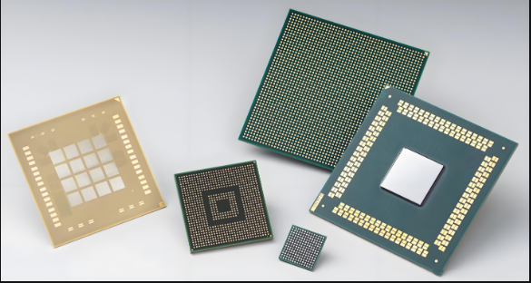
In modern PCB design, bottom-pad packages such as BGA, CSP, and QFN are increasingly common. The solder joints of these components are covered by the package body and cannot be inspected visually or by AOI, requiring an X-ray system.
X-ray can detect: voids in BGA solder balls; short circuits or unsoldered solder balls; via filling conditions in multilayer PCBs (Via-in-Pad process); and internal cracks or delamination issues in solder joints.
This is an indispensable inspection step for high-frequency boards, automotive electronics, and military equipment.
In-Circuit Test (ICT)
ICT is the most commonly used electrical testing method in the assembly industry, suitable for medium to high volume production.
ICT can detect: whether components are correctly soldered; whether resistors, capacitors, and inductors have excessively large deviations; whether there are open circuits or short circuits; and whether the basic functions of ICs are normal.
Advantages include:
High speed, high accuracy, and coverage of most functional points on a PCB.
Disadvantages:
Requires specialized fixtures; high cost for small batches.
Therefore, ICT is typically used in high-volume products such as large consumer electronics and automotive electronics.
Functional Test (FCT)
Unlike ICT, FCT focuses on overall functional verification and is a testing method that simulates real-world usage scenarios.
FCT does:
Power-on testing, reading or programming chip programs, monitoring input/output signals, simulating user operations, and verifying product functions (such as sensors, communication modules, signal outputs, etc.). Almost all electronic products must undergo FCT before leaving the factory to ensure stable operation.
Design for Manufacturability (DFM) in Assembly
Assembly quality depends not only on the manufacturing process but also on the PCB design stage; therefore, DFM is crucial in board PCB assembly.
Common design issues affecting PCBA quality include:
Improper pad design leading to cold solder joints; insufficient BGA spacing and unreasonable routing; vias placed in pads without filler; excessively narrow spacing between surface-mount components; uneven heat dissipation across different layers.
Many PCBA manufacturers provide a Design FM Report after receiving a Gerber order to help customers identify potential design flaws early and reduce assembly risks.
Industry Quality Standards and Certification Systems
High-reliability PCB assembly typically requires compliance with the following industry standards:
IPC-A-610 Class II/III: Industry standard for electronic assembly; Class III is used for medical, aerospace, and high-reliability equipment.
ISO 9001: Basic Quality System
IATF 16949: Automotive Electronics
UL certification: Safety certification
RoHS/REACH environmental standards
Stringent industry certifications mean stricter process control and lower failure rates.
Application Scenarios of Board PCB Assembly in Major Industries
With the rapid development of electronic technology, Board PCB Assembly (PCB Assembly) has been widely used in almost all industries involving electronic control, signal processing, and power management. From consumer to industrial, from high-speed communications to medical and automotive electronics, the quality and stability of PCBAs directly affect the lifespan and performance of end products. This chapter will systematically describe the practical application scenarios and technical requirements of Board PCB Assembly in several key industries.
Communication and High-Speed Network Equipment
In the fields of 5G, optical communication, and high-speed data exchange, PCBAs need to possess the following characteristics:
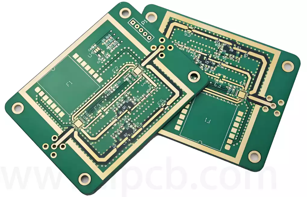
Support for high-speed signal transmission (10–100Gbps), reliable soldering of ultra-low-loss materials (such as PTFE, Rogers, and Megtron series), high-density packages such as BGA and QFN, multi-layer or even HDI structures, and support for complex RF links.
Common products include: base station motherboards, optical modules, routers, and switches.
These devices have extremely high requirements for assembly accuracy and signal integrity; therefore, PCBA factories need to have advanced mounting capabilities and a rigorous testing system.
Industrial Control and Automation Equipment
Industrial equipment typically operates in harsh environments, requiring PCBAs with higher tolerance to temperature, humidity, and vibration.
Typical products include: PLC control boards, servo drives, sensor modules, and power supply modules.
These scenarios place the following demands on PCBAs:
High-reliability soldering and long lifespan; high heat resistance and insulation; mixed assembly processes with numerous through-hole components (THT); and more stringent functional testing (FCT) processes.
Industrial-grade assembly emphasizes stability rather than extreme miniaturization.
Automotive Electronics. Automotive electronics is rapidly expanding, from traditional ECUs to ADAS, vehicle radar, BMS, motor controllers, and various other modules, all relying on highly reliable PCBAs.
Automotive electronics are characterized by: mandatory compliance with IATF 16949 standards; a wide operating temperature range (-40°C to 125°C); vibration resistance; strong anti-interference capabilities; increased use of thick copper plates; high current design; and extremely high functional safety requirements (ISO 26262). Even minor assembly defects can affect vehicle safety.
Medical electronics. Medical devices have extremely high requirements for precision and stability. Board PCB assembly must be performed in a clean environment with strictly controlled temperature and humidity.
Common products include: ECG monitors, ultrasound equipment, portable point-of-care testing (POCT) devices, and vital sign monitoring devices.
Requirements typically include:
High-precision and zero-tolerance assembly, compliance with IPC-A-610 Class III, and rigorous FCT and aging tests. Medical electronics require PCBAs to be “zero-risk, zero-error.”
Consumer electronics. Consumer electronics is the most active market for PCBAs, including smart wearables, Bluetooth speakers, smart home devices, and small appliances.
The key characteristics are:
Short product lifecycle, high-volume rapid delivery, high-density placement, miniaturized design, and high requirements for appearance inspection and consistency.
PCBA factories typically need high-speed placement lines to support large-volume orders.
Different application scenarios have vastly different requirements for Board PCB Assembly, but the core objective remains the same—ensuring safe, stable, and reliable electronic performance. For PCBA factories, only by continuously improving engineering capabilities, reliability testing capabilities, and process control levels can they truly meet the diverse needs of the modern electronics industry.
Summary
As electronic technology continues to mature, board PCB assembly is no longer simply a process of “soldering components onto a circuit board,” but a system engineering project integrating material selection, structural design, assembly processes, testing and verification, and quality control. From pad layout to high-speed signal optimization, from automated placement to functional testing, the professionalism at each step directly affects the stability and market competitiveness of the final product.
In the context of the current structural upgrade of the electronics industry, the role of PCBAs is becoming increasingly crucial: the communications industry relies on them for high-speed interconnection; automotive electronics need them to support safety and reliability; medical devices require them to provide high-precision, error-free operation; and consumer electronics use them to achieve thinner, lighter, and smarter experiences. The demands of different application scenarios are driving board-level assembly technology towards higher density, lower loss, and higher reliability.
The future of board PCB assembly will rely more heavily on automated production, intelligent testing, and process innovation. Excellent suppliers will not only need to solve processing problems but also possess engineering capabilities, collaborative abilities, and a deep understanding of industry standards. In short, whoever masters advanced assembly technology will gain an advantage in the next era of electronics manufacturing.