Ceramic multilayer PCBs (printed circuit boards) represent a unique and highly specialized type of circuit board used in various industries requiring exceptional reliability, high-frequency performance, and durability. Unlike traditional PCBs that typically use materials like FR4, ceramic multilayer PCBs leverage the properties of ceramic materials to achieve superior thermal management, electrical performance, and mechanical strength. This article will explore the key features, benefits, applications, and manufacturing process of ceramic multilayer PCBs.
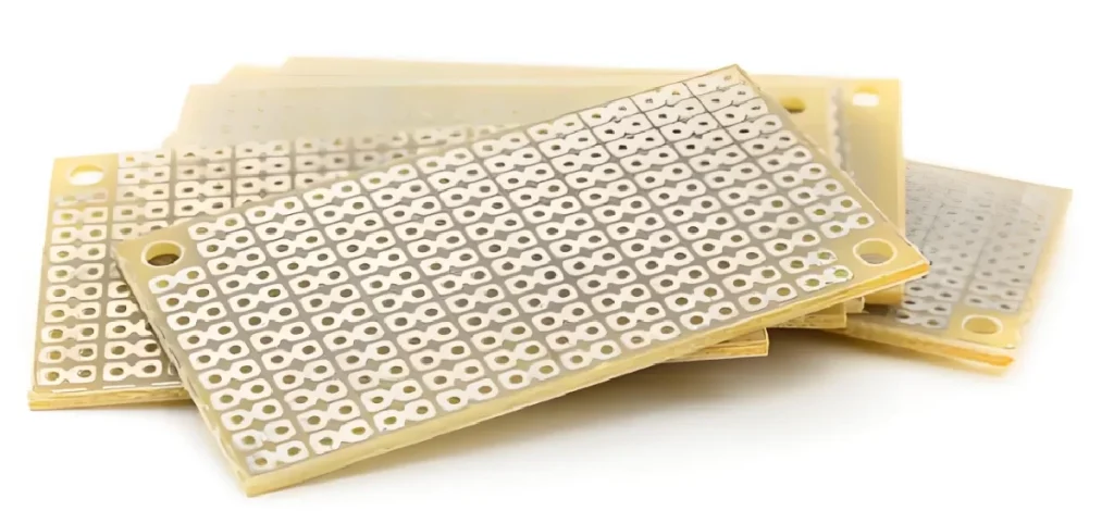
What Is a Ceramic Multilayer PCB?
A ceramic multilayer PCB is a type of printed circuit board made using ceramic materials, such as alumina (Al2O3), aluminum nitride (AlN), or beryllium oxide (BeO), as the substrate. These materials are known for their excellent thermal conductivity, low dielectric constant, and high thermal stability, making them ideal for applications where traditional PCB materials might fall short.
The construction of a ceramic multilayer PCB involves stacking multiple layers of ceramic material, each layer containing its circuit patterns. These layers are then laminated together and co-fired, meaning they are subjected to high temperatures to form a single, cohesive structure. The result is a PCB that can operate in harsh environments, handle high power levels, and maintain performance in high-frequency applications.
Key Benefits of Ceramic Multilayer PCBs
- Exceptional Thermal Management
One of the most significant advantages of ceramic multilayer PCBs is their superior thermal management capabilities. Ceramic materials, such as aluminum nitride and alumina, have high thermal conductivity, which allows them to efficiently dissipate heat generated by electronic components. This feature is particularly valuable in applications like power electronics, RF amplifiers, and LED lighting, where excessive heat can significantly impact performance and longevity. - High-Frequency Performance
Ceramic multilayer PCBs are known for their excellent performance in high-frequency applications. The low dielectric constant of ceramic materials helps reduce signal loss and maintains signal integrity at high frequencies. This makes ceramic multilayer PCBs ideal for use in RF and microwave circuits, radar systems, and communication devices where maintaining signal fidelity is critical. - Mechanical Strength and Reliability
The inherent mechanical strength of ceramic materials makes ceramic multilayer PCBs highly durable and reliable, even in extreme conditions. These PCBs can withstand high levels of mechanical stress, thermal cycling, and exposure to harsh chemicals, making them suitable for aerospace, automotive, and military applications. The robust nature of ceramic multilayer PCBs ensures they can operate in environments where traditional PCBs would likely fail. - Miniaturization and Integration
Ceramic multilayer PCBs enable the miniaturization of electronic devices by allowing for the integration of multiple functions into a single, compact board. The ability to stack multiple layers of circuits within a small footprint makes these PCBs an excellent choice for applications where space is at a premium. This feature is particularly advantageous in the medical device industry, where compact and highly reliable electronics are essential. - Environmental Stability
Ceramic multilayer PCBs are inherently stable in a variety of environmental conditions. They exhibit minimal expansion or contraction with temperature changes, making them suitable for applications where dimensional stability is critical. This property is particularly beneficial in optical devices and sensors, where precision is paramount.
Applications of Ceramic Multilayer PCBs
Ceramic multilayer PCBs find applications in various industries, particularly where high performance, reliability, and durability are paramount.
- Aerospace and Defense
In aerospace and defense, where electronics are exposed to extreme temperatures, vibrations, and other harsh conditions, ceramic multilayer PCBs offer the reliability and robustness needed. They are commonly used in radar systems, communication devices, and guidance systems, where their high-frequency performance and durability are critical. - Medical Devices
The medical industry benefits from ceramic multilayer PCBs due to their ability to support miniaturization and integration. These PCBs are used in implantable devices, diagnostic equipment, and high-precision instruments where reliability and compactness are crucial. The biocompatibility of certain ceramic materials also makes them suitable for use in medical applications. - Automotive Electronics
Automotive electronics require PCBs that can withstand high temperatures, vibrations, and exposure to chemicals. Ceramic multilayer PCBs are used in engine control units, sensors, and power electronics in electric vehicles, where their thermal management capabilities and durability make them ideal. - Telecommunications
The telecommunications industry relies on ceramic multilayer PCBs for high-frequency and high-power applications. These PCBs are used in RF amplifiers, filters, and other components in communication systems that demand low signal loss and high reliability. - Industrial Electronics
In the industrial sector, ceramic multilayer PCBs are utilized in power electronics, sensors, and control systems that operate in demanding environments. These PCBs can handle high current loads, resist chemical exposure, and maintain performance under mechanical stress, making them a preferred choice for heavy-duty applications. - Optoelectronics
Optoelectronic devices, such as lasers and photodetectors, benefit from the dimensional stability and thermal management properties of ceramic multilayer PCBs. The precision required in these devices makes ceramic PCBs an ideal substrate, ensuring consistent performance in optical communication and measurement systems.
Manufacturing Process of Ceramic Multilayer PCBs
The manufacturing of ceramic multilayer PCBs is a complex and precise process that involves several key steps:
- Material Selection and Preparation
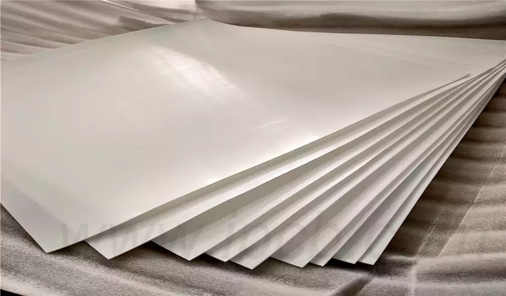
The process begins with selecting the appropriate ceramic material based on the desired thermal and electrical properties. Common materials include alumina, aluminum nitride, and beryllium oxide. The ceramic material is typically prepared in a slurry form, which is then cast into thin sheets or tapes. - Circuit Layer Printing
Once the ceramic layers are prepared, the circuit patterns are printed onto each layer using a thick-film or thin-film process. Thick-film printing involves screen printing conductive, resistive, and dielectric pastes onto the ceramic substrate. Thin-film printing, on the other hand, uses photolithography to create finer circuit patterns. The choice of process depends on the application requirements and the desired level of precision. - Lamination and Co-firing
After the circuit patterns are printed, the individual ceramic layers are stacked in the desired order and laminated together. The laminated stack is then co-fired at high temperatures, causing the layers to fuse into a single, solid structure. This step is critical in ensuring the mechanical integrity and electrical performance of the final PCB. - Via Formation and Metallization
Vias, or interconnects, are created between the layers to allow electrical connections between the different circuit patterns. This is typically done using laser drilling or mechanical drilling, followed by filling the vias with conductive material, usually a metal paste. The vias are then metallized to ensure proper electrical conductivity. - Surface Finishing
The surface of the ceramic multilayer PCB is often finished with a protective layer to enhance durability and performance. This finishing process may include the application of solder mask, protective coatings, or metallization layers, depending on the intended application. Surface finishing also helps to protect the circuits from environmental factors such as moisture and corrosion. - Final Inspection and Testing
The final step in the manufacturing process involves inspecting the ceramic multilayer PCB for defects, such as voids, misalignments, or short circuits. The PCB is then tested for electrical performance, including continuity, insulation resistance, and signal integrity. Quality control is crucial to ensure the PCB meets the required specifications and performs reliably in its intended application.
Challenges in Ceramic Multilayer PCB Manufacturing
While ceramic multilayer PCBs offer numerous benefits, their manufacturing process presents several challenges that must be addressed to achieve optimal performance.
- Material Handling
The ceramic materials used in multilayer PCBs can be brittle and challenging to handle during the manufacturing process. Careful attention must be paid to material preparation, cutting, and lamination to prevent cracking and ensure uniformity. - Precision Requirements
The need for high precision in circuit patterning and via formation requires advanced manufacturing techniques and equipment. Any misalignment or deviation can result in poor electrical performance or mechanical failure. As such, manufacturers must maintain stringent quality control measures throughout the production process. - Cost Considerations
The use of specialized materials and processes in ceramic multilayer PCB manufacturing can result in higher production costs compared to traditional PCBs. While the benefits often justify the cost in high-performance applications, manufacturers must carefully consider cost-benefit trade-offs when selecting ceramic multilayer PCBs for specific projects. - Thermal Management
Although ceramic multilayer PCBs excel in thermal management, the co-firing process used to fuse the layers can introduce thermal stress. Manufacturers must carefully control the firing temperature and duration to avoid warping, delamination, or other thermal defects.
Conclusion
Ceramic multilayer PCBs represent a significant advancement in PCB technology, offering unmatched thermal management, high-frequency performance, and mechanical strength. Their ability to operate in harsh environments and support the miniaturization of electronic devices makes them indispensable in industries such as aerospace, defense, medical devices, automotive electronics, telecommunications, industrial electronics, and optoelectronics.
The manufacturing process of ceramic multilayer PCBs is intricate and requires precise control over material selection, circuit printing, and lamination to achieve the desired performance characteristics. Despite the complexity, the benefits of ceramic multilayer PCBs make them a preferred choice for applications where reliability and high performance are non-negotiable.
As electronic devices continue to evolve, the demand for ceramic multilayer PCBs is expected to grow, driven by the need for more compact, reliable, and high-performing circuits. Understanding the unique properties, applications, and challenges associated with ceramic multilayer PCBs is essential for engineers, designers, and manufacturers looking to leverage this advanced technology in their products.
