Wafer Level Packaging (WLP) is an advanced packaging technology that has developed rapidly in recent years due to its advantages of small size, excellent electrical performance, good heat dissipation and low cost.
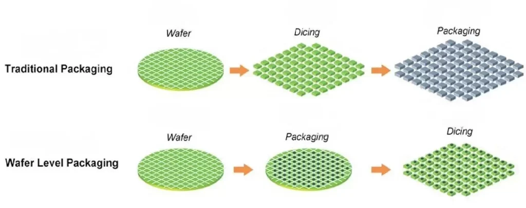
Different from the traditional packaging process, wafer level packaging is in the chip is still on the wafer when the chip is encapsulated, the protective layer can be glued to the top or bottom of the wafer, and then connected to the circuit, and then cut the wafer into individual chips.
Wafer-level packaging technology and playing line type (Wire-Bond) and Flip-Chip (Flip-Chip) packaging technology compared to the elimination of playing metal wires, epitaxial pins (such as QFP), substrates or lead frames and other processes, so the package has a small size, good electrical performance advantages. Packaging industry leaders are mostly based on the wafer model to mass produce advanced wafer-level packaging products, not only can use the existing wafer-level manufacturing equipment to complete the operation of the main packaging process, but also to make the package structure, chip layout design parallel to become a reality, which significantly shortens the design and production cycle, reducing the overall project cost.
In traditional wafer packaging, the finished wafer is cut into individual chips and then glued package. Unlike the traditional packaging process, wafer-level packaging is in the chip is still on the wafer when the chip is encapsulated, the protective layer can be glued to the top or bottom of the wafer, and then connected to the circuit, and then cut the wafer into individual chips.
Wafer-level packaging has the advantages:
1, small package size
As there is no lead, bonding and plastic process, the package does not need to expand to the outside of the chip, making the package size of the WLP is almost equal to the chip size.
2, high transmission speed
Compared with traditional metal-lead products, WLP generally have a shorter connection line, in high performance requirements such as high frequency, there will be a better performance.
3, High density connection
WLP can utilize array connection, the connection between the chip and the board is not limited to the chip around, improve the connection density per unit area.
4, short production cycle
WLP from the chip manufacturing to, packaging to the finished product of the whole process, the intermediate links are greatly reduced, high production efficiency, the cycle is much shorter.
5, Low process cost
wafer-level packaging is completed at the wafer level packaging testing, batch production to achieve the goal of cost minimization. the cost of WLP depends on the number of qualified chips on each wafer, chip design size reduction and wafer size increase in the development trend of single device packaging cost is reduced accordingly. the WLP can make full use of wafer fabrication equipment, production facilities, low cost.
It should be emphasized that, unlike wire bonding, wafer-level packaging uses wafer-level packaging technology to achieve intracavity signal routing (Internal Signal Routing), there are several options: wafer-level bumping (Wafer Bumping) technology, redistribution layer (Re-Distribution Layer) technology, Silicon Interposer technology, Through Silicon Via technology, and so on. Silicon Interposer) technology, silicon perforation (Through Silicon Via) technology.
Advanced wafer-level packaging technology, including five major elements:
① wafer-level bumping (Wafer Bumping) technology;
② Fan-in (Fan-In) wafer-level packaging technology;
③ Fan-out (Fan-Out) wafer-level packaging technology;
④2.5D wafer-level packaging technology (including IPD);
⑤3D wafer-level packaging technology (including IPD).
Wafer Bumping, as the name suggests, is the formation or installation of solder balls (also known as bumps) in a predetermined position on a wafer before cutting it. Wafer Bumping is a key technology to realize the interconnection between chips and PCBs or substrates. The selection of materials, construction, and dimensional design of bumps are influenced by a variety of factors, such as package size, cost, and electrical, mechanical, and thermal performance requirements.
Printed Bump, Ball Drop with Eutectic Plating, Lead-Free Alloy and Copper-Pillar Alloy, Fan-In Wafer Level Package (FIWLP). Wafer Level Package (FIWLP) technology, also known in the industry as wafer level chip scale package (Wafer Level Chip Scale Package, WLCSP) technology, is today’s various types of wafer level packaging technology in the main force. In the past two years, fan-in wafer-level packaging products, global shipments have remained at more than 30 billion per year, mainly for cell phones, smart wearable and other portable electronic products market.
The development trend of wafer-level packaging:
With the continuous upgrading of electronic products, smart phones, 5G, AI and other emerging markets put forward higher requirements for packaging technology, making packaging technology toward highly integrated, three-dimensional, ultra-detail distance interconnection and other directions. Wafer-level packaging technology can reduce the chip size, wiring length, solder ball spacing, etc., so you can improve the integration of integrated circuits, processor speed, etc., to reduce power consumption, improve reliability, in line with the increasingly thin and lightweight electronic products, short, low-cost development needs.
With the shrinking space of portable electronic products, increasingly high operating frequency and the diversification of functional requirements, the number of chip input/output (I/O) signal interfaces has increased significantly, the bump and ball pitch (Bump Pitch & Ball Pitch) of the degree of precision requirements are becoming increasingly stringent, and the mass production yield of the redistributed layer (RDL) technology is also therefore more and more attention. Against this background, Fan-Out Wafer Level Package (FOWLP) and Hybrid Fan-In/Fan-Out have emerged as high-end wafer level packaging technologies.
Whether focusing on the present, or looking into the future, with 5G, artificial intelligence, the Internet of Things and other major technology trends coming, in the high-density heterogeneous integration of the technology race, wafer-level packaging technology is bound to occupy a place.