HDI PCB stands for High Density Interconnector printed circuit board, which represents high-density interconnect printed circuit board. Compared to traditional circuit boards, this type of circuit board is designed to have higher density interconnect circuits and components..
In today’s era of high-performance, miniaturization, and lightweight electronic devices, HDI PCB technology has become the core of the electronic manufacturing field. By optimizing circuit layout and material application, HDI circuit boards have achieved higher density of circuit connections, further improving the performance of electronic devices.
At present, there are 5 main types of HDI PCB: 1-order HDI, 2-order HDI, 3-order HDI, 4-order HDI, and Anylayer HDI PCBs. The size gradually decreases from front to back, making manufacturing more difficult. At present, electronic terminal products mainly use 3-order, 4-order, and Anylayer HDI, while high-end smartphones mainly use 3-order HDI boards with 10 or more layers. The higher the order, the more pressing times are required.
What is the difference between HDI PCB and FR-4 PCB?
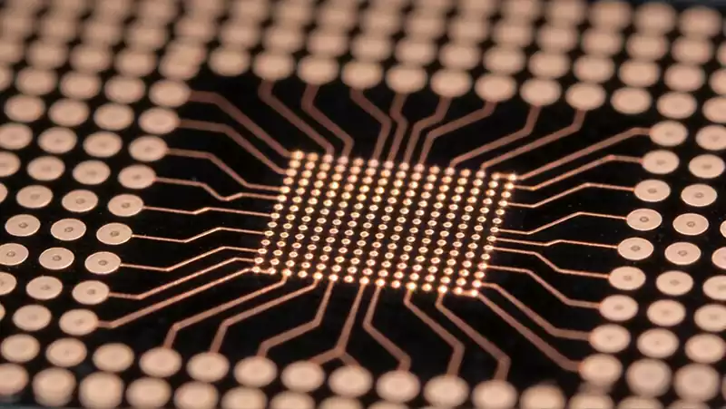
Micropores: HDI PCB utilize micropores, which are small and compact holes drilled on the board, allowing for more interconnection without taking up too much space. Microvias can be stacked to create multi-layer interconnections.
Fine pitch: HDI PCB support fine pitch components with small pad sizes, allowing more components to be placed in smaller areas.
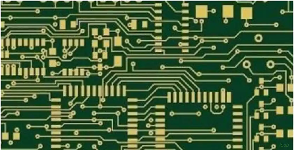
High layer count: Compared to traditional circuit boards, HDI PCB can have higher layers, allowing for more routing choices and improved circuit performance.
High density circuits: HDI PCB have density circuits that increase interconnectivity, reduce the need for long signal paths, and enhance signal integrity.
Multi order: HDI circuit board use multiple buried and blind holes to form a multi order circuit board, resulting in a higher circuit density.
Advantages of HDI PCB technology
The core of HDI PCB lies in its unique circuit layout and material application, enabling more and denser circuit connections in limited space. Compared with circuit board, it has significant advantages.
High Integration: By optimizing the circuit layout, high density interconnect pcb achieve higher density of circuit connections, increasing the integration of electronic devices.
High reliability: In fact, the line connection ensures the reliability and stability of signal transmission, reducing the risk of failure.
High performance: suitable for high-speed, big data rate signal transmission, meeting the high-performance requirements of modern electronic products.
Miniaturization and lightweighting: allowing for smaller dimensions and lighter weight, enhancing product portability and aesthetics.
Low cost: Although the manufacturing process is relatively complex, its efficient production methods and material utilization have reduced costs.
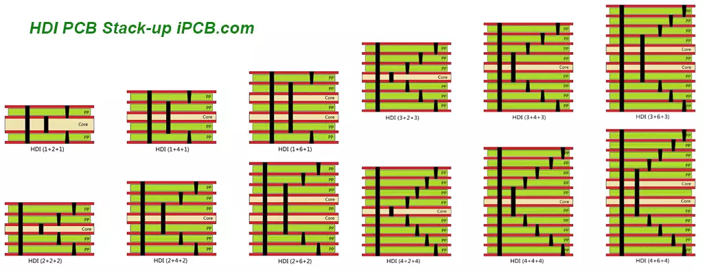
HDI PCB Stack-up
HDI circuit boards are usually divided into 1+N+1, 2+N+2, 3+N+3, 4+N+4, 5+N+5, 6+N+6, and Anylayer HDI. Numbers represent the number of times blind holes need to be manufactured, and the current maximum manufacturing capacity of iPCB is 6th order. N represents buried holes, and Anylayer HDI PCB represents all blind holes.
This stacking method includes the top layer, middle layer, and bottom layer. The top layer is usually used to place solder pads for components, the middle layer is used to place power and ground wires, and the bottom layer is the wiring area for signal wires. The main advantage of this stacked structure is that it can effectively reduce signal interference and improve the quality of signal transmission.
High density interconnect pcb manufacturing process
Design circuit diagram: Use electronic design automation (EDA) software to create circuit diagrams and optimize the layout to meet high-density wiring requirements.
Production of inner layer: The inner layer is made by laminating thin copper foil onto the substrate or using a stacked lamination process. These internal layers will be used to implement complex interconnect structures.
High precision drilling: Use laser drilling machines to accurately drill micro holes. These holes will be used for electrical connections between internal layers.
Electroplated hole wall: After drilling, a thin layer of copper is electroplated on the hole wall to form a reliable conductive path.
Adding Copper Clad Layer: Add laminated materials and copper coated layers between the internal layers to form a multi-layer PCB structure. Each layer has copper foil for electrical connections.
Graphical patterning: Use UV light to scrape off unprotected copper foil areas and form circuit patterns.
Pads and Printing: Add pads and printing for soldering components.
Surface treatment: Surface treatment is carried out where necessary, such as metalization, anti-corrosion treatment, or protective coating.
Component installation: Install components onto HDI PCBs using surface mount technology (SMT) or insertion technology.
Testing and Inspection: Test and inspect the manufactured HDI PCB to ensure that the circuit is working properly and there are no short circuits or other issues.
Packaging and delivery: The completed HDI PCB will be packaged and delivered to the customer as required or further integrated into the final product.
HDI PCBs are widely used in communication, computer, military and other fields. In the field of communication, it is used to build high-performance communication equipment, such as base stations and routers. In the field of computer motherboards, it has become the preferred choice for high-performance computer hardware. In the military field, it is used for military equipment such as missile guidance systems and radar systems. In addition, fields such as medical equipment and industrial control systems also benefit from the application of HDI circuit boards. Taking smartphones as an example, due to their miniaturization and high performance requirements, HDI circuit boards have become an ideal choice for internal wiring connections, enhancing the performance and user experience of the phone.
With the continuous development of technology, HDI PCB circuit board technology will continue to improve and progress. In the future, it will develop towards higher performance, lower costs, and more environmentally friendly directions. In addition, with the emergence of new technologies such as 5G communication and the Internet of Things, the application areas will further expand. As an advanced technology in the field of electronic manufacturing, HDI PCB will become the preferred electronic manufacturing technology for smartphones, IoT devices, and other high-tech products due to its excellent performance and low cost advantages.