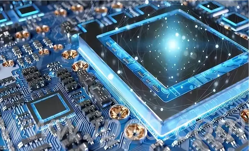
Introduction to PCB Panel Design
Printed Circuit Board (PCB) panel design is a critical aspect of electronic manufacturing, significantly influencing the efficiency, cost, and quality of the production process. This article delves into the essential principles and practices of PCB panel design, offering comprehensive insights into the subject.
Importance of PCB Panel Design
The significance of PCB panel design lies in its ability to streamline the manufacturing process. Proper panel design minimizes waste, reduces handling time, and improves yield rates. It ensures that multiple PCBs can be processed simultaneously, leading to more efficient use of production resources.
Key Considerations
Panel Size and Shape
The size and shape of the panel are primary considerations. Standard panel sizes often conform to industry norms to maximize compatibility with manufacturing equipment. However, custom sizes may be necessary for specific applications. The shape must allow for optimal placement of the individual PCBs to maximize material usage and minimize waste.
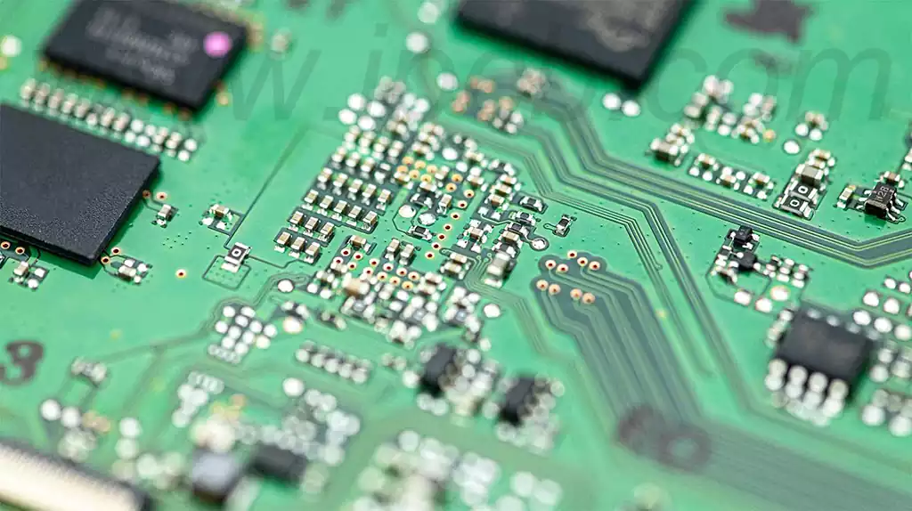
Component Placement and Orientation
Strategic placement and orientation of components on the PCB panel are crucial. Components should be placed in a manner that facilitates efficient soldering and assembly. The orientation should be consistent across the panel to ensure uniformity in manufacturing processes such as wave soldering or reflow soldering.
Tooling Holes and Fiducials
Tooling holes and fiducials are essential for alignment and registration during the manufacturing process. Tooling holes are used to secure the panel during various stages of production, ensuring precise positioning. Fiducials, on the other hand, serve as reference points for automated assembly equipment, aiding in accurate component placement.
Breakaway Tabs and V-Scoring
Breakaway tabs and V-scoring are techniques used to separate individual PCBs from the panel after assembly. Breakaway tabs are small sections of the panel left attached to the PCB, which can be easily broken off after assembly. V-scoring involves making shallow cuts along the edges of the PCBs, allowing them to be snapped apart with minimal effort.
Copper Balance
Copper balance refers to the even distribution of copper across the PCB panel. Uneven copper distribution can lead to warping during the manufacturing process. Ensuring a balanced copper layout is essential to maintain the flatness of the panel, which is critical for accurate assembly and soldering.
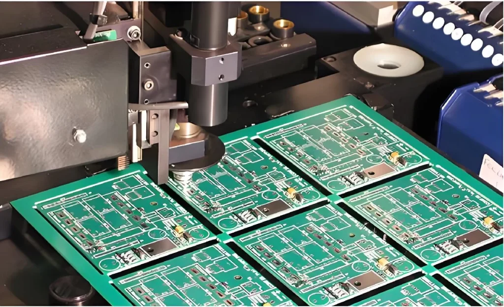
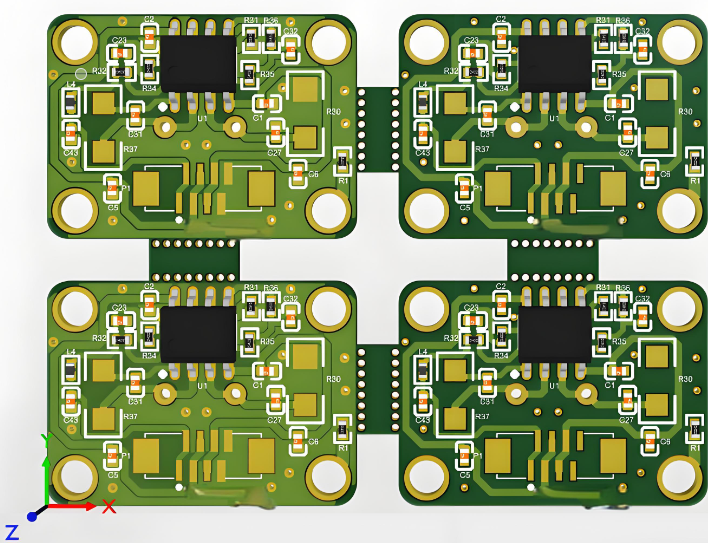
Panelization Methods
Several panelization methods are used in PCB manufacturing, each with its advantages and disadvantages.
Grid panelization involves arranging PCBs in a grid pattern on the panel. This method is simple and efficient, making it suitable for high-volume production. However, it may not be ideal for complex board shapes or layouts.
Array panelization allows for more flexible arrangement of PCBs on the panel, accommodating various shapes and sizes. This method is beneficial for low to medium-volume production runs and for PCBs with irregular shapes.
Combination PanelizationCombination panelization involves mixing different PCB designs on a single panel. This method maximizes material usage and reduces costs, especially for small-volume production runs. However, it requires careful planning to ensure compatibility of the different designs.
Design for Manufacturability (DFM)
Design for Manufacturability (DFM) is a crucial aspect of PCB panel design. DFM principles aim to optimize the design for ease of manufacturing, reducing the likelihood of defects and improving overall yield. Key DFM considerations include:
Minimize Component Variability
Using standard component sizes and types reduces variability in the manufacturing process, making it easier to achieve consistent results. It also simplifies inventory management and reduces the risk of component shortages.
Optimize Trace Routing
Efficient trace routing minimizes the length and complexity of connections between components, reducing the risk of signal integrity issues and improving the overall performance of the PCB.
Ensure Adequate Clearances
Adequate clearances between components and traces are essential to prevent shorts and ensure reliable operation. DFM guidelines typically specify minimum clearance distances to be maintained.
Consider Thermal Management
Effective thermal management is critical to prevent overheating and ensure the longevity of the PCB. Incorporating thermal vias, heat sinks, and adequate spacing between heat-generating components are essential aspects of thermal management.
Advanced Panel Design Techniques
High-Density Interconnect (HDI) Panels
High-Density Interconnect (HDI) technology allows for the design of PCBs with higher component densities and finer trace widths. HDI panels enable the production of more compact and complex designs, suitable for modern electronic devices such as smartphones and tablets.
Flex and Rigid-Flex Panels
Flex and rigid-flex panels offer greater design flexibility by combining rigid and flexible PCB materials. These panels are ideal for applications requiring complex geometries and dynamic bending, such as wearable electronics and medical devices.
Embedded Components
Embedding components within the PCB substrate can significantly reduce the overall size and weight of the final product. This technique is particularly useful for miniaturized devices where space is at a premium.
Challenges in PCB Panel Design
Design Complexity
As the complexity of electronic devices increases, so does the complexity of PCB panel design. Designers must navigate a myriad of constraints, including signal integrity, thermal management, and mechanical stability, to achieve optimal performance.
Manufacturing Variability
Variability in the manufacturing process can lead to defects and inconsistencies. Designers must account for potential variations in material properties, process parameters, and equipment capabilities to ensure reliable production.
Cost Considerations
Balancing cost and performance is a perpetual challenge in PCB panel design. Designers must make trade-offs between material costs, manufacturing complexity, and product performance to achieve a cost-effective solution.
Time-to-Market Pressure
The competitive nature of the electronics industry demands rapid development cycles. Designers must work efficiently to meet tight deadlines while maintaining high standards of quality and reliability.
Future Trends in PCB Panel Design
Automation and AI
Advancements in automation and artificial intelligence (AI) are poised to revolutionize PCB panel design. AI algorithms can optimize panel layouts, predict potential defects, and suggest design improvements, significantly reducing design time and improving yield rates.
Advanced Materials
The development of advanced materials, such as conductive polymers and nanomaterials, offers new possibilities for PCB design. These materials can enhance the electrical, thermal, and mechanical properties of PCBs, enabling more sophisticated and reliable products.
Internet of Things (IoT)
The proliferation of IoT devices is driving demand for highly integrated and miniaturized PCBs. Designers must innovate to meet the unique requirements of IoT applications, including low power consumption, wireless connectivity, and robust performance in diverse environments.
Sustainable Design
Environmental sustainability is becoming increasingly important in PCB panel design. Designers are exploring eco-friendly materials, energy-efficient manufacturing processes, and end-of-life recycling solutions to reduce the environmental impact of electronic products.
Conclusion
PCB panel design is a complex and multifaceted discipline, critical to the success of electronic manufacturing. By understanding the key principles and considerations, designers can create efficient, cost-effective, and high-quality PCB panels. As technology continues to evolve, advancements in materials, automation, and design techniques will further enhance the capabilities and possibilities of PCB panel design, driving innovation in the electronics industry.