The Fundamental Concepts and Core Position of Copper Clad Laminate PCBs
In the entire electronics manufacturing industry, copper clad laminate (CCL) is one of the most core and fundamental materials constituting a PCB (Printed Circuit Board). A laminate PCB board refers to a printed circuit board made primarily of copper clad laminate, formed through multiple processes including vacuum hot pressing, etching, drilling, and electroplating. The quality of the CCL directly determines the PCB’s electrical performance, mechanical strength, processing stability, and reliability in various application environments such as high temperature, high humidity, and high frequency. Therefore, it is considered the foundation of electronic product performance.
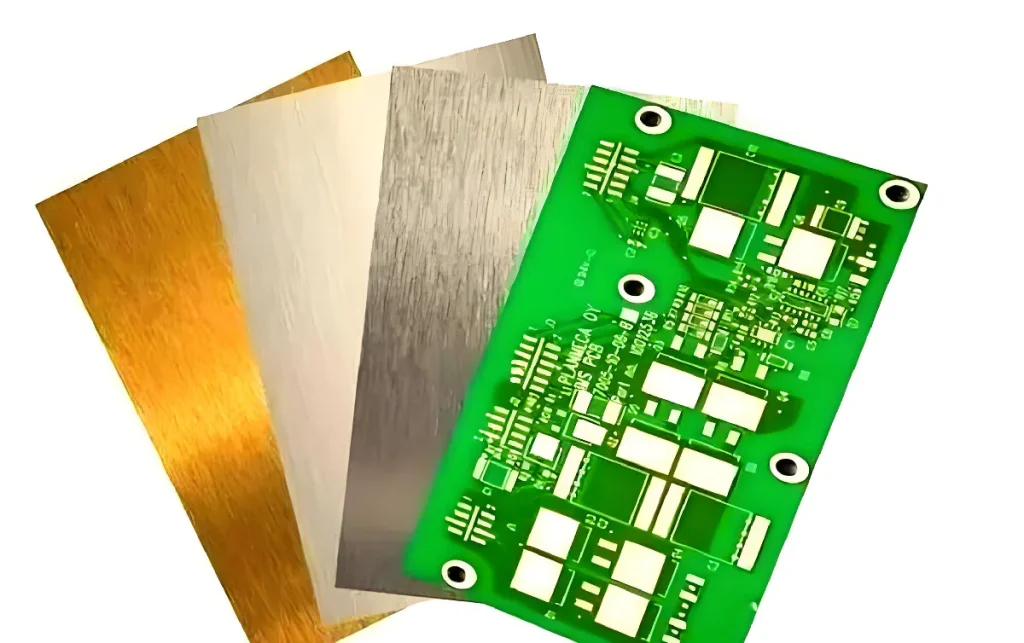
CCLs typically consist of three main parts: a resin system, reinforcing materials, and copper foil. The resin system provides electrical insulation and dielectric properties; its formulation affects key parameters such as heat resistance, water absorption, and dielectric constant. The reinforcing materials provide structural strength and stability, with fiberglass cloth being the most common choice. The copper foil, as the conductor layer, is the carrier for circuit signal transmission. After hot pressing, these three components form a stable layered structure that resists stress, ensures dimensional accuracy, and prevents warping or delamination during processing.
Copper clad laminates (CCLs) come in a wide variety of types, primarily classified based on factors such as resin system, dielectric constant, thermal properties, and mechanical characteristics. The most commonly used is FR4 CCL, suitable for most consumer electronics and low-to-mid-range industrial control applications. High-frequency, high-speed equipment requires materials with low dielectric loss, such as PTFE series, ceramic-filled resin boards, and hybrid-structured boards. In addition, there are high-temperature resistant PI CCLs, metal-based CCLs, high CTI flame-retardant series, and high-reliability materials suitable for harsh environments such as automotive. Each type of CCL has its typical applications and performance advantages.
As electronic products continue to evolve towards miniaturization, high speed, and high reliability, the role of CCLs is becoming increasingly crucial. For example, in 5G communication equipment, high signal frequencies and stringent loss control requirements necessitate materials with low dielectric loss (Dk), low dielectric loss (Df), and extremely high dimensional stability. In automotive radar and new energy equipment, CCLs require comprehensive characteristics such as high heat resistance, impact resistance, and high reliability. In consumer electronics, manufacturing cost, processability, and stability become the main considerations for material selection.
Therefore, when we discuss laminated PCBs, we are actually discussing a complete system of fundamental engineering that determines the performance of electronic products. Materials are not simply stacked; rather, it’s a dynamic balance across three dimensions: electrical performance, mechanical performance, and process window. The dielectric constant of the material affects signal speed, dielectric loss affects signal attenuation, copper foil roughness determines insertion loss in high-speed circuits, and resin content and fiberglass cloth pattern determine heat resistance, warpage, and even the reliability of high-layer boards.
More importantly, copper-clad laminates not only affect the performance of the final product but also profoundly impact the manufacturing process. Drilling conditions, electroplating adhesion, lamination flow, and CTE matching of different materials can all cause deviations in a process, thus affecting the yield rate. Therefore, a high-quality copper-clad laminate is not just a material product but also a crucial guarantee for the stability of the entire manufacturing chain.
There’s a saying in the industry: “Good material selection is half the battle won in PCB development.” This is no exaggeration for high-reliability and high-performance applications. Behind almost any high-end electronic product, you can find a meticulously designed copper-clad laminate structure. Therefore, understanding the characteristics and functions of copper-clad laminates is fundamental to understanding the entire PCB.
Material Composition and Manufacturing Principles of Laminate PCB Boards
The core of laminate PCB board manufacturing lies in the composition of the material system and the principle of multilayer lamination. This process determines whether the PCB can operate stably in complex electrical and mechanical environments. Therefore, before understanding copper-clad laminate materials, it is necessary to analyze them from four fundamental dimensions: resin system, reinforcing materials, copper foil characteristics, and lamination process, as these are the initial sources of performance for all electronic devices.
Let’s start with the resin system. Resin is the electrical insulation basis of copper-clad laminates. Common systems include epoxy resin, modified resin, high-frequency resistant resin, ceramic filler systems, and multifunctional composite resins. Epoxy resin is the mainstream choice for most FR4 type copper-clad laminates due to its moderate cost and balanced properties; however, in high-speed and high-frequency scenarios, PTFE, hydrocarbon resin, or ceramic hybrid systems with lower dielectric constants and dielectric losses are required. The resin system directly affects the thermal properties of the board material, including Tg (glass transition temperature), Td (thermal degradation temperature), and CTE (coefficient of thermal expansion). These parameters are crucial because they determine whether the board will delaminate during welding, whether it will expand excessively at high temperatures, and whether fatigue cracks will appear during repeated thermal cycling.
Reinforcing materials are the source of structural strength. The most common material in the industry is glass fiber cloth, with weaves including 7628, 2116, and 1080, to match different resin contents and flow requirements. For weight reduction or enhanced heat resistance, special structures such as non-woven fabrics, aramid fibers, and ceramic fibers are also used. The choice of reinforcing material not only affects mechanical strength but also the resin flow and filling effect during lamination. Especially in multilayer board structures, the stability of the glass fiber cloth is key to ensuring consistent interlayer dielectric thickness.
Copper foil serves as the carrier of the conductive network, and its quality and surface morphology play a decisive role in high-speed circuits. Copper foil with higher roughness exhibits stronger adhesion but increases signal loss; while ultra-low roughness copper foil (VLP, HVLP) is suitable for high-speed circuits because it reduces insertion loss for high-speed signals. The thickness of the copper foil also affects trace width, current carrying capacity, and heat dissipation performance; for example, common thicknesses of 1oz, 2oz, and 3oz are used for different current ratings; special applications such as power modules and automotive electronics may even use copper plates thicker than 6oz. The purity of the copper foil, the electrolysis method, and organic surface treatments (OSP, zinc plating, brown plating) all affect subsequent etching and lamination adhesion.
Once these materials are ready, the copper-clad laminate manufacturing process begins. Lamination is the core process, fusing resin, fiberglass cloth, and copper foil into a single unit using high temperature, high pressure, and vacuum. During lamination, the resin needs to be heated to a sufficient flow stage and then cured above its glass transition temperature to form a stable structure. The uniformity of resin flow, the amount of resin flowing, the curing rate, and the matching relationship with the fiberglass cloth are crucial. Inconsistencies can lead to dielectric thickness errors, voids, delamination, or warping.
Furthermore, during the manufacturing of laminated PCB boards, the lamination profile must be strictly controlled, including the heating rate, holding time, vacuum level, and cooling process. These parameters affect whether the resin is fully cured, whether internal stress occurs, and whether the interlayer is smooth. For high-speed boards, the resin curing system is more complex, requiring multi-stage curing to ensure molecular chain stability; while for thick copper boards, extra attention needs to be paid to resin filling capacity to avoid voids and insufficient resin caused by uneven copper foil thickness.
After lamination, a copper-clad laminate blank is formed, but it is not the final usable PCB material. It still needs to be cut, surface treated, visually inspected, and subjected to performance testing. Performance tests include withstand voltage, insulation resistance, dielectric constant, water absorption rate, and thermal stress testing; each directly affects the reliability of the final PCB. For example, materials with excessively high water absorption can cause changes in dielectric constant in humid and hot environments, affecting signal stability; materials with poor thermal stress performance are prone to delamination during wave soldering; and materials with high dielectric loss cannot meet the requirements of 5G high-frequency applications.
For manufacturers, material processability is also crucial. While some high-performance resin systems offer excellent electrical properties, they are difficult to drill, prone to resin shrinkage or hole wall cracking, posing significant challenges to production. Therefore, material selection must consider not only performance but also the factory’s ability to perform the corresponding processes.
In summary, laminate PCB board is not merely a material stacking process, but an engineering challenge involving a balance between electrical performance, processability, and mechanical strength. Material formulation, lamination methods, and structural design collectively determine the final PCB performance, which is why different types of copper-clad laminates must be used for different application environments.
Electrical Characteristics and Performance Influence Mechanisms of Laminate PCB Boards
When designing and using laminate PCB boards, electrical performance is often one of the core factors that engineers are most concerned about. Especially with the continuous development of electronic devices towards higher speeds, miniaturization, and high-frequency communication, factors such as the dielectric constant, dielectric loss, insulation properties, and surface structure of copper foil have been pushed to the forefront of influencing system performance. A stable and high-quality copper-clad laminate (CCL) must maintain signal integrity, suppress losses, reduce crosstalk, and maintain consistency in interlayer electrical characteristics under harsh environments. The following will analyze the electrical characteristics and influencing mechanisms of CCL from multiple dimensions.
The dielectric constant (Dk) is one of the most critical indicators for evaluating the electrical performance of materials. The level of Dk directly affects signal propagation speed; the lower the Dk, the faster the signal. Simultaneously, the stability of Dk also determines the impedance consistency of the circuit. In high-speed digital circuits, RF front-ends, antenna design, and high-speed transmission links, the Dk of materials must maintain extremely high consistency. Since the interior of a copper-clad laminate is composed of resin, fiberglass cloth, and fillers, Dk will exhibit slight variations due to differences in material proportions, fabric structure, and resin distribution. These variations can be amplified infinitely in high-speed signals, leading to impedance deviations. Therefore, high-quality laminate materials must possess extremely low dielectric loss (Dk) tolerances, and dielectric stability can be improved by optimizing the fiberglass cloth pattern and resin impregnation method.
Dielectric loss (Df) determines the degree of energy loss during signal propagation within the dielectric. With continuously increasing data transmission rates, signal loss has become one of the key bottlenecks affecting performance. In applications such as 5G communications, radar systems, high-performance servers, and high-speed backplanes, lower Df results in better signal quality. Traditional FR4 materials, due to their high dielectric loss, are unsuitable for high-speed applications; while low-loss materials such as ceramic-filled resins, PTFE series, and hydrocarbon resins exhibit greater stability. It is worth noting that although some materials have extremely low Df, they are difficult to process and costly; therefore, material selection during product development often requires a balance between electrical performance and manufacturing feasibility.
Besides the electrical properties of the dielectric itself, the surface roughness of the copper foil also significantly affects signal integrity. When high-speed signals propagate on the copper foil surface, they are affected by the skin effect, causing the current to tend to distribute on the outer layer of the conductor surface. If the copper foil surface is too rough, the signal path becomes tortuous and uneven, resulting in a longer propagation path and increased transmission loss. Therefore, in high-speed and high-frequency applications, finely processed low-roughness or ultra-low-roughness copper foil is essential. This type of copper foil not only significantly reduces transmission loss but also improves the stability of the line impedance, contributing to improved signal integrity of the overall link.
Water absorption rate is also an extremely important electrical parameter. The lower the water absorption rate, the more stable the dielectric constant of the material in humid environments. High water absorption rate materials will experience an increase in Dk and a deterioration in Df due to moisture penetration, ultimately leading to signal attenuation, impedance changes, and even insulation failure. Low water absorption rate materials are crucial in outdoor equipment, automotive electronics, and high-reliability communication systems that are constantly exposed to temperature and humidity changes. Therefore, high-end copper-clad laminates typically employ denser resin formulations and uniform fiberglass cloth impregnation processes to enhance resistance to moisture.
Insulation performance is related to reliability and safety. The insulation resistance, withstand voltage, and arc resistance of the material determine its stability in high-voltage applications. For example, in applications such as power modules, energy equipment, and industrial drives, materials must not only withstand high voltages but also resist prolonged charging and discharging, as well as instantaneous shocks. Inferior materials may experience leakage or dielectric breakdown. Therefore, in high-power systems, copper-clad laminate materials with high insulation levels and high withstand voltage are required.
Heat dissipation performance is also a crucial factor affecting electrical performance. As power density in circuits continues to increase, relying solely on air convection for heat dissipation is no longer sufficient. The thermal conductivity of materials has a significant impact on overall heat dissipation efficiency, especially in applications with high heat generation, such as power modules, LED light sources, and RF PA modules. Poor heat dissipation can lead to electrical performance degradation, accelerated aging, and even thermal runaway. Therefore, some laminate materials incorporate ceramic fillers or thermally enhanced resins to improve thermal conductivity, allowing devices to operate at more stable temperatures.
Furthermore, the stability of electrical performance is also affected by the uniformity of the material structure. Uneven resin content distribution, fiberglass cloth corrugations, and variations in copper foil adhesion can all cause localized minor differences. While these differences have little impact in low-speed circuits, in high-speed links, even minor deviations can cause signal reflection, delay errors, and increased bit errors. Therefore, high-quality copper-clad laminates employ more precise coating control systems, more advanced fiberglass cloth weaving technology, and stricter monitoring of lamination parameters during production to ensure consistency of the final material at both the macroscopic and microscopic levels.
Overall, the quality of electrical performance not only determines the final performance of the system but also affects the controllability of the design and the tolerance of manufacturing. A stable and reliable laminate PCB board must strike a balance between dielectric properties, conductor properties, environmental adaptability, and process compatibility to maintain consistent performance over long-term operation. As the electronics industry continues to move towards higher frequencies, higher speeds, and higher reliability, the electrical performance of materials will become one of the core competitive advantages and an important foundation that cannot be ignored in research and development and manufacturing.
Key Points of Laminate PCB Board Manufacturing Process and Quality Control
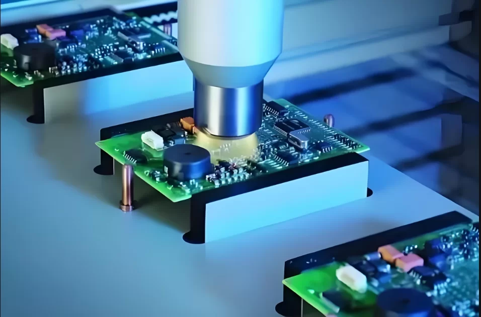
The manufacturing of laminate PCB boards is not simply a matter of cutting, drilling, and etching copper-clad laminates; it is a highly precise and systematic process. Each step in the manufacturing process directly determines the dimensional stability, electrical performance, and long-term reliability of the finished product. For PCBs with different layers and material systems, even minor deviations during manufacturing can lead to problems such as interlayer misalignment, impedance drift, delamination, or warping. Therefore, understanding the manufacturing process and quality control logic of laminate boards is crucial to ensuring their performance stability and batch consistency.
First, the lamination process is the core step in the entire laminate board production. It combines multiple layers of prepreg (PP) and copper foil into a single unit under high temperature and pressure. This process not only requires sufficient resin flow and uniform distribution but also necessitates control over the curing reaction. Lamination parameters such as heating rate, maximum temperature, pressure profile, and cooling rate all affect the final resin distribution and interlayer bonding strength. If the temperature rises too quickly, the resin may gel prematurely, leading to insufficient flow and the formation of voids or resin-depleted areas.
If cooling is too slow, internal stress can easily develop, leading to board warping or delamination. Therefore, in high-reliability PCB manufacturing, manufacturers often use automated temperature-controlled presses and set independent hot-pressing profiles for each layer to ensure consistent thermosetting resin reaction and fiberglass cloth impregnation.
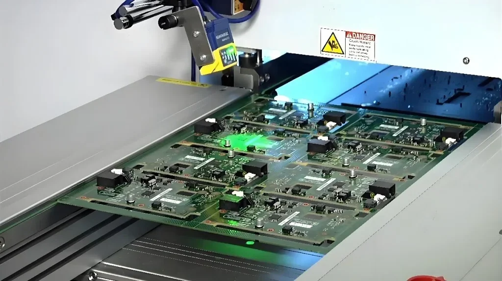
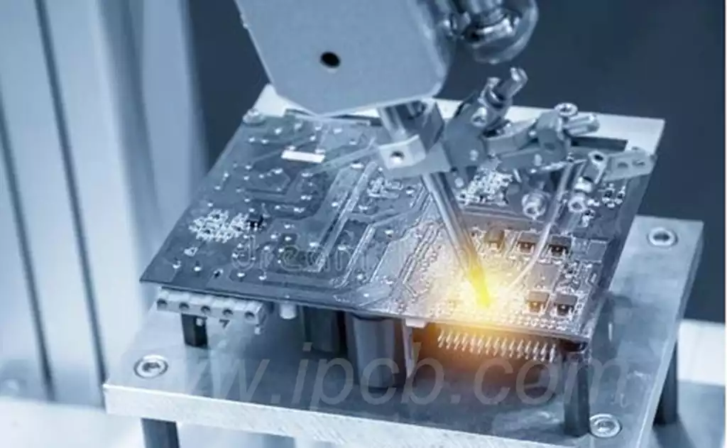
Secondly, there is the drilling process, which connects the conductive structures between layers. As the number of layers increases, thickness varies, and fiberglass density rises, drilling precision and hole wall quality become crucial. While standard mechanical drilling can be used for ordinary FR4 materials, high-end laminate boards containing ceramic or high-Tg resin systems require high-speed drills, micro-diameter drill bits, and specialized chip removal control strategies. If the drilling speed is mismatched, burrs on the hole walls, resin tearing, or fiberglass fraying can easily occur, affecting electroplating quality. Therefore, high-end manufacturing lines are typically equipped with automatic compensation systems that automatically adjust the feed rate and tool wear compensation based on material hardness and thickness to ensure the smoothness and dimensional consistency of each through-hole.
Electroplating of the hole walls after drilling is a crucial step in establishing conductivity. The uniformity of the copper plating layer determines the reliability and thermal shock resistance of the via. Typically, a chemically deposited copper (PTH) base is used, followed by electrolytic copper plating for thickness enhancement. The PTH stage requires uniform activation and a stable chemical solution; otherwise, discontinuous plating on the hole walls will occur. The electroplating stage requires controlling the current density distribution through a rectification system, stirring flow rate, and anode layout to ensure consistent plating thickness. Especially in high-layer boards, the current distribution in deep-hole electroplating is extremely complex. Improper control can result in an excessively thin plating layer at the bottom of the hole, creating a hidden reliability risk. Therefore, reputable manufacturers employ pulse plating or reverse plating techniques to achieve a denser and more uniform plating layer at the microscopic level.
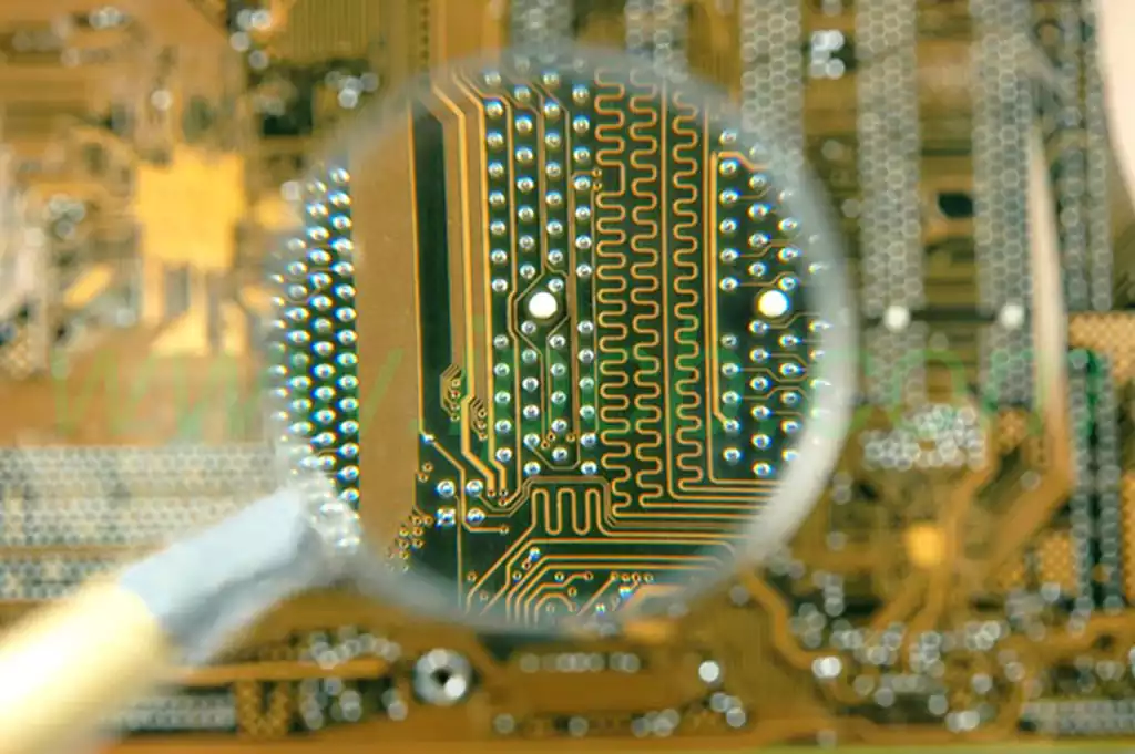
Next is the etching process, which uses chemical etching to remove unwanted copper foil, forming the circuit pattern. As circuit density increases and line width and spacing decrease, the control requirements for etching become increasingly stringent. The etching solution concentration, temperature, spray pressure, and time must be precisely matched; otherwise, “side etching” or “under-etching” can easily occur, leading to deviations in the circuit shape. Especially in high-frequency applications, even minute changes in edge morphology can alter characteristic impedance. Therefore, modern etching equipment employs closed-loop concentration monitoring systems and automatic flow regulation to maintain a constant etching rate, ensuring circuit consistency and geometric accuracy.
Quality control is the heart of the entire laminate PCB board manufacturing process. After lamination, interlayer alignment detection, X-ray calibration, and microscopic section analysis are performed to confirm the parallelism and symmetry of each copper foil layer and dielectric. The drilling and electroplating stages require through-hole copper thickness detection, SEM surface scanning, and thermal stress testing to verify via reliability. After etching, AOI (Automated Optical Inspection) is performed to check for circuit defects, broken lines, short circuits, and burrs. Finally, the finished board undergoes flying probe testing or electrical performance testing to ensure all signal paths are connected and impedance meets design requirements.
Throughout the entire production chain, material pretreatment is also a crucial step in ensuring quality. Before entering the production line, copper-clad laminates must undergo baking and dehumidification to prevent moisture absorption that could lead to delamination or bubbles. The copper foil surface must be roughened or blackened to improve adhesion. The PP layer must be stored in a constant temperature and humidity environment to prevent premature resin reaction or fluctuations in moisture content. Even during the visual inspection stage, microscopic observation and interlayer scanning are required to ensure the absence of microcracks, interlayer bubbles, and impurity residue.
It is worth emphasizing that with the increasing automation of manufacturing, data-driven quality management is gradually becoming a trend. Advanced factories use MES (Manufacturing Execution System) to record key parameters such as temperature, pressure, chemical concentration, and current density in real time, and analyze fluctuation trends using Statistical Process Control (SPC) methods to prevent defects from occurring in advance. This data-driven quality system not only improves yield but also significantly enhances product consistency and traceability, becoming a hallmark of high-end PCB manufacturing.
In summary, the manufacturing of laminated PCB boards is a highly systematic and precise engineering process. From lamination to drilling, from electroplating to etching, from inspection to traceability, every step affects the performance of the final product. Only through rigorous process control, meticulous testing systems, and continuous process optimization can every circuit board meet the expected standards in terms of structure, electrical properties, and reliability. This deep-seated process control capability is also an important indicator of a PCB manufacturer’s overall strength.
Application Areas and Development Trends of Laminate PCB Boards
Laminate PCB boards are widely used in almost all areas of the electronics and information industry. Their performance directly determines the stability and lifespan of end devices. In consumer electronics, they are the foundational material for smartphones, tablets, and wearable devices, undertaking high-speed signal transmission and multi-layer interconnection tasks. In communication equipment, especially in 5G base stations, optical modules, and high-speed routers, low-loss, high-stability high-frequency copper-clad laminates are crucial for signal integrity. Automotive electronics also rely heavily on high-performance laminate boards, used in core control components such as ECUs, radar systems, battery management units, and new energy inverter modules, where requirements for high-temperature resistance and shock resistance are particularly stringent.
In industrial control and medical equipment, the reliability and environmental resistance of laminate PCB boards determine the stability of the system during long-term operation. For example, industrial control computers, robot control boards, ultrasonic equipment, and monitoring instruments all require precise signal response in humid, high-temperature, or vibration environments. Furthermore, with the rise of aerospace and new energy fields, the demand for special laminate boards with high Tg, high withstand voltage, and low dielectric loss has increased significantly. Materials such as ceramic-based copper-clad laminates and PTFE hybrid systems are gradually replacing traditional FR4 to meet applications under higher frequencies and more extreme temperature conditions.
Looking ahead, the development trends of laminate PCB boards mainly focus on three aspects: high frequency and high speed, green sustainability, and functional integration. With the improvement of AI computing power and high-speed communication, signal transmission rates will continue to increase, making the demand for low dielectric constant and low-loss materials even more prominent. At the same time, the promotion of environmental regulations has made halogen-free, low-carbon emission, and recyclable resin systems a research focus. On the other hand, manufacturing technology is evolving towards “structure and function integration,” such as directly embedding heat dissipation layers, magnetic materials, or sensing units into copper-clad laminates, making the PCB not only a circuit carrier but also an integral part of system functionality.
Summary
laminate PCB boards are at the core of electronic manufacturing technology innovation. They are not only the cornerstone supporting the modern electronics industry but will continue to play an irreplaceable role in the future high-performance, intelligent electronic world.
In conclusion, as the most fundamental and critical material system in the electronics manufacturing industry, the importance of laminate PCB boards has long surpassed the definition of “circuit carrier.” They not only support signal transmission, energy distribution, and structural support in modern electronic devices but also, through continuously evolving material technologies and manufacturing processes, drive the entire industry towards higher frequencies, higher speeds, and higher reliability. From the refined improvement of resin systems to the precise control of copper foil morphology; from the optimization of multilayer lamination process parameters to the introduction of automated quality management systems, every technological advancement is reshaping the performance limits of laminate boards.
Looking to the future, the trends of miniaturization, intelligence, and high power in electronic products will continue to drive the development of copper-clad laminates (CCLs) towards higher thermal conductivity, lower loss, and lighter weight. The application of new materials such as fluoropolymers, ceramic composite systems, and low-roughness copper foil is constantly breaking through the performance bottlenecks of traditional FR4. Meanwhile, automated and digital manufacturing, along with data-driven quality control, is transforming the PCB industry from experience-based manufacturing to precision engineering.
In short, laminated PCBs are not only the physical foundation of electronic manufacturing but also a vital source of industrial innovation. They embody the combined achievements of materials science, mechanical manufacturing, and signal engineering, connecting the microscopic electronic world with the macroscopic industrial system. Regardless of future technological advancements, the progress of CCLs will continue to drive the core pulse of the electronics industry.