Introduction and Clarification
In the electronics manufacturing industry, printed circuit boards (PCBs) are fabricated using a variety of methods. Milling, as a key process, is gaining increasing attention from companies and engineers. Milling PCB Board involves using CNC milling equipment to cut and process the PCB along a pre-defined path, ultimately achieving the desired shape and contour. This method differs from traditional die stamping or simple V-cut separation, offering greater flexibility and precision to meet customized needs.
Understanding this process is essential for a comprehensive understanding of the PCB manufacturing process. As electronic products evolve toward thinner, smaller, and more precise designs, milling is becoming a crucial tool for meeting the demands of high-end PCB fabrication.
Compared to traditional stamping, milling does not rely on expensive molds and is more suitable for small batches and complex PCB shapes. Compared to laser cutting, milling offers advantages in processing thicker boards and ensuring edge squareness. Its flexibility and stability make it a key component of the PCB fabrication process. Furthermore, with the widespread adoption of CNC technology, the automation level of milling continues to improve, ensuring consistent and repeatable processing and further reducing the risk of human error.
From a broader industry perspective, PCB milling is more than just a process; it actually reflects the transformation and upgrades PCB manufacturers are undergoing in response to market demand. Whether it’s smartwatches in consumer electronics, sensor modules in medical devices, or control units in automotive electronics, a growing number of applications require PCBs with fine edges and complex shapes, and milling perfectly fills this need.
Understanding PCB milling is a key to understanding the “flexibility and precision” of modern PCB manufacturing. It not only helps companies shorten R&D cycles but also provides downstream customers with greater design freedom.
Process Principles and Equipment Introduction
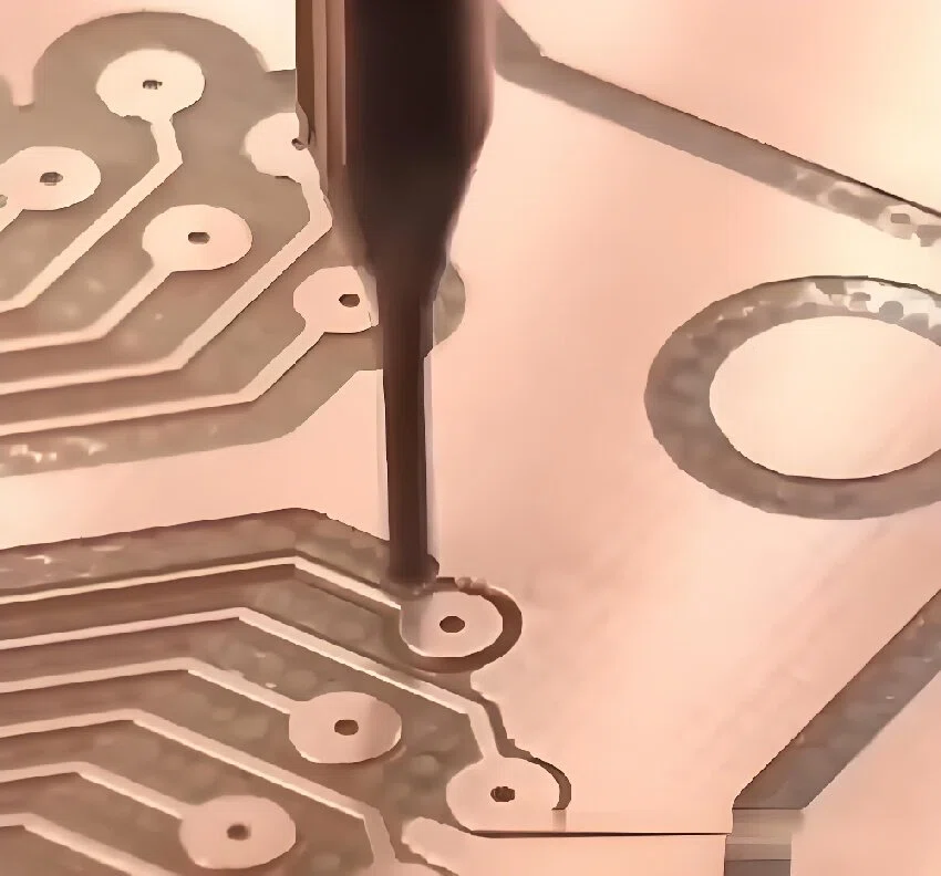
The core of PCB milling lies in “subtractive machining,” whereby CNC milling equipment (CNC routers) transforms a regular, large-scale PCB panel into a specific shape, slot, or sub-panel configuration according to design requirements. Similar to drilling, milling also relies on a high-speed rotating tool to remove material, but differs in that it focuses more on creating two-dimensional contours and complex geometries.
Process Principle
The basic principle of milling involves using a high-speed spindle to drive a carbide tool to cut into the FR4 substrate or flexible copper-clad laminate of a PCB. The tool follows a pre-set CNC program path, removing unwanted areas and ultimately leaving the desired circuit board outline and structure. The entire process relies on a path file generated by CAD/CAM software (usually Gerber data combined with a CNC program) to achieve precise alignment between design and machining.
During the machining process, tool selection, spindle speed, and feed rate are three key parameters that influence the quality of the finished product. Excessively high feed rates can lead to burrs and chipped edges, while too low can result in inefficient machining and even burnt material. Therefore, experienced engineers will select the appropriate tool diameter and cutting strategy based on the board thickness, copper layer weight, and design complexity. For example, when machining thick plates, multiple cuts are typically made in layers, while when machining thin or flexible boards, the cutting depth needs to be reduced to avoid warping.
Equipment Components
Modern PCB milling equipment is mostly high-precision CNC milling machines, typically consisting of the following core components:
Spindle system: The spindle speed typically ranges from 60,000 RPM and above, ensuring stable and smooth cutting.
Tool system: Carbide tools are primarily used, with diameters ranging from 0.6mm to 3.0mm. Some high-end models are equipped with automatic tool changing systems that automatically switch between tools of different diameters during machining.
Worktable and fixture: Used to secure the PCB panel to prevent vibration and misalignment during machining. Some machines also support vacuum suction to further improve machining accuracy.
CNC control system: Path control is performed using G-code or a dedicated CNC program to ensure tool movement is consistent with the design files.
Dust Removal and Cooling System: The cutting process generates a large amount of dust, which must be collected using efficient dust removal equipment. Furthermore, for thick plates or long processing times, air or water cooling is required to prevent overheating.
Influence of Process Parameters
Spindle Speed: Higher speeds produce smoother cut edges, but also increase tool wear.
Feed Speed: Too high a speed can easily lead to edge chipping, while too low a speed can affect efficiency; a balance must be found.
Tool Diameter: Smaller diameters produce finer details, but tool life is relatively short.
Depth of Cut: Layered cutting helps reduce burrs and stress concentrations, which is particularly crucial in thick plate processing.
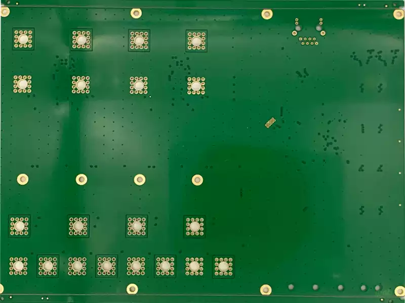
Through appropriate equipment configuration and process parameter control, milling PCB boards can achieve extremely high dimensional accuracy (typically within ±0.1mm tolerances), meeting customer requirements for complex shapes and precise slots.
Application Scenarios and Advantages
The importance of milling PCB boards in PCB manufacturing lies in its ability to address requirements that are difficult to meet using traditional molding methods. As electronic products continue to become smaller, more complex, and more powerful, the application of milling technology is expanding.
Small-Batch Production and Rapid Prototyping
For foreign trade buyers and R&D engineers, the initial stages of product development often require only a few dozen or even a few PCBs. Using stamping requires custom molds for each design, which is both costly and time-consuming. Milling, on the other hand, eliminates the need for molds; engineers simply input the design files into a CNC system for complete production. This significantly shortens the R&D cycle and lowers the barrier to entry for small-batch production. Many startups and innovative projects rely on milling to quickly produce product prototypes.
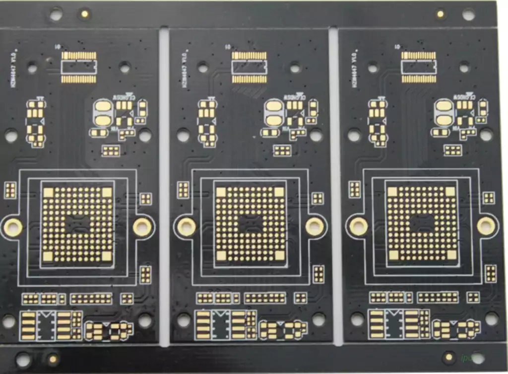
Complex Shapes and Special Slot Processing
In modern electronic products, many circuit boards are no longer traditional rectangular shapes. Instead, they incorporate complex features such as rounded corners, irregular edges, internal grooves, and notches. For example, sensor modules in medical devices and control units in electric vehicles often require the integration of specially designed PCBs into limited space. Stamping processes lack flexibility, while milling allows for precise, designed routing, ensuring a secure fit between the finished product and the housing or module.
Industries Demanding High Precision
In automotive electronics, industrial control, and aerospace, the contour accuracy and edge quality of PCBs directly impact the reliability of the entire device. Milling PCBs can guarantee machining accuracies of ±0.1mm or higher, while avoiding the cracks and stress concentrations that can occur with V-cut processes. Milling is particularly critical for boards that need to be installed inside precision machinery.
Integration with Flexible Circuits and Multilayer Boards
The manufacturing process of multilayer and flexible PCBs often requires grooving, chamfering, and cutting complex contours. Milling not only achieves high-precision machining on rigid FR4 materials, but also allows for the shaping of flexible PCBs using low-speed, shallow cuts, avoiding the tearing and warping common with traditional processes. This compatibility makes milling PCBs a key processing method for integrated manufacturing plants.
Balancing Cost and Efficiency
While milling may not be as cost-effective as die stamping for high-volume production, it offers excellent value for money in small and medium-volume production. Customers do not incur additional die costs; manufacturers only need to maintain the tools and equipment. Especially during product development with frequent revisions, the flexibility of milling can help customers significantly reduce R&D costs while maintaining rapid iteration.
Arguably, the greatest advantage of milling PCBs lies in its “combination of flexibility and precision.” It can meet the personalized needs of R&D and prototyping while providing a stable and reliable molding solution for high-end applications. In many cases, it has become more than just a supplementary process; it has become a vital foundation for driving innovation in electronics manufacturing.
Process Challenges and Technical Difficulties
Despite the flexibility and high precision of milling PCBs, there are still several technical difficulties in actual processing. Understanding these challenges is crucial for engineers to optimize the process and improve the quality of the finished product.
Burrs and Edge Chipping
During the milling process, burrs and edge chipping are easily generated when the tool cuts through the PCB substrate and copper layers at high speeds. Burrs not only affect the appearance but can also cause subsequent soldering or assembly problems, even resulting in short circuits or poor contact. Chipping is particularly problematic on thick PCBs or PCBs with large copper layers. Solutions include:
Using multiple shallow cuts instead of a single deep cut to reduce stress concentration; selecting sharp and wear-resistant carbide tools to ensure cutting sharpness; and adjusting feed rates and spindle speeds for smooth cutting and reduced material drag.
Tool Wear and Life Management
Machining high-density, multi-layer boards, or thick copper plates can accelerate tool wear. Tool wear not only reduces machining accuracy but can also cause burrs or edge defects in critical areas. Engineers typically need to plan tool changes based on material type, copper thickness, and cutting frequency, and increase cooling and lubrication measures during high-load machining to extend tool life.
Challenges in Machining Thick and Multi-Layer Boards
When machining multi-layer PCBs or thick copper plates, milling tools must precisely control cutting depth; otherwise, delamination between layers, board warping, or local shorts can occur. Furthermore, the inner copper foil of multi-layer boards may pull out or deform during cutting, affecting overall reliability. Therefore, process design often incorporates layered cutting, edge supports, and specialized fixtures to ensure stability of each layer.
Thermal Stress and Material Warpage
The high-speed rotation of the tool during milling generates heat, especially on thick boards or PCBs with high copper thickness. This localized temperature rise can easily cause thermal expansion and warping of the material. This deformation affects dimensional accuracy and edge perpendicularity. To address this, intermittent cutting, reduced feed rates, and the use of cooling air or liquid cooling systems can be used to control the temperature rise.
Processing Limitations Due to Design Complexity
Some designs contain sharp corners, tiny through-holes, or internal slots that the milling tool may not be able to reach directly or could easily damage the board. In these cases, optimizing the tool path, adding auxiliary cuts, or fine-tuning the design are necessary to ensure process feasibility. Furthermore, close communication between engineers and the design team during the prototype phase to ensure that the design is compatible with process capabilities is crucial to reducing failure rates.
Compatibility Issues with Other Processes
PCB milling is typically not performed in isolation; it is often combined with processes such as drilling, copper cladding, and V-cutting. Different processes have different requirements for board thickness, edge quality, and mechanical strength. Improper coordination can cause dimensional deviations or damage the copper foil. Solutions include:
Establishing unified process specifications to clarify the processing sequence and parameters; conducting multiple trial runs during the prototype phase to verify the compatibility of various processes;
Strengthening the fixing or support of key areas to prevent damage during subsequent processes.
In summary, the challenges of milling PCB boards primarily focus on burrs, chipping, thermal stress, tool wear caused by physical cutting, and the complexity of multilayer board processing. Through appropriate tool selection, cutting strategies, fixture design, and process parameter optimization, these difficulties can be largely overcome, ensuring the accuracy and reliability of the final PCB.
Quality Control and Inspection Methods
After milling PCB boards, ensuring that the finished product meets design requirements is a crucial step in the PCB manufacturing process. Strict quality control not only ensures product reliability but also enhances customer trust in suppliers.
Dimensional Accuracy Inspection
After milling a PCB, the first step is to check whether the board’s dimensions are consistent with the design. Common methods include:
Calipers and coordinate measuring machines (CMMs): Used to measure PCB length, width, hole and slot positions, achieving high accuracy requirements of ±0.05mm.
Optical projectors: Through high magnification and image measurement, they can quickly determine whether edge profile deviations or burrs exist.
Accurate dimensional inspection is particularly important for complex shapes, internal grooves, or high-density multi-layer boards to ensure interference-free subsequent assembly and installation.
Edge finish inspection
Milling can easily cause burrs, chipping, or microcracks. These defects can escalate into more serious problems during welding or vibration environments. Therefore, edge finish inspection is necessary:
Microscope inspection: Magnifies critical areas to identify burrs and edge damage.
Scanning electron microscopes (SEMs): Used for high-precision PCBs to detect microcracks and copper delamination.
If edge defects are found, deburring, micro-polishing, or secondary milling can be used to repair them.
Material Integrity Testing
Multi-layer boards or thick copper boards are prone to interlayer delamination or copper foil damage after milling. Inspection methods include:
X-ray inspection: This can check for delamination, short circuits, or microcracks between internal layers.
Electrical continuity testing: Using a multimeter or automated testing equipment, the conductivity and insulation of each circuit are checked to ensure circuit integrity.
Compatibility Testing with Other Processes
Milling PCBs often requires integration with processes such as drilling, copper cladding, or V-cut separation. Quality control requires inter-process compatibility checks:
Confirm that the milling edge does not conflict with the drill hole location to ensure mechanical strength;
Check that the slot depth and angle meet subsequent assembly requirements;
Mark and track boards that have undergone multiple processes to avoid quality issues caused by sequencing errors.
Automated Inspection and Data Recording
With the development of smart manufacturing, more and more PCB manufacturers are incorporating automated inspection into the milling process:
Visual Recognition Systems: Leveraging high-definition cameras and image recognition software, these systems automatically scan edges, holes, and slots to quickly detect deviations or burrs.
Data Tracking Systems: These systems correlate inspection results with processing parameters and tool usage to create a complete quality record, facilitating traceability and improvement.
Systematic inspection and quality control not only ensures the dimensional accuracy and edge quality of milled PCBs, but also provides customers with traceable, verifiable, and highly reliable products.
Development Trends and Intelligent Directions
With the rapid development of the electronics industry, milling PCBs is moving beyond traditional, low-volume processing and is evolving towards high-precision, intelligent, and automated processes. Understanding these trends can help companies and engineers proactively plan their design and manufacturing processes and enhance their competitiveness.
Automation and High-Precision CNC Technology
Modern PCB milling equipment generally utilizes CNC (computer numerical control) technology, enabling high-precision, repeatable machining. In the future, these equipment will be further enhanced with:
High-speed spindles and micro-tools: enabling the machining of smaller and more detailed PCB features;
Multi-axis machining: supporting complex angles, beveled slots, and irregular shapes, reducing manual operations;
Automatic tool changing and online calibration: automatically monitoring and replacing tool wear to ensure consistent machining.
The development of automation not only improves production efficiency but also reduces human error, making the manufacturing of small-batch, highly complex PCBs more reliable.
Intelligent Inspection and Data-Driven
Intelligent manufacturing concepts are being integrated into the milling PCB production process:
Real-time monitoring systems: sensors monitor tool status, cutting temperature, and vibration, enabling timely adjustment of process parameters;
Machine vision and AI inspection: automatically identifying edge burrs, cracks, and deviations, enabling high-speed, accurate inspection;
Data feedback and optimization: combining machining data with quality inspection results to form a closed-loop optimization loop and continuously refine milling strategies.
This intelligent trend is gradually transforming PCB manufacturing from experience-driven to data-driven, improving reliability and traceability.
Green Manufacturing and Environmentally Friendly Materials
With the promotion of sustainable development concepts, the environmental impact of PCB processing is gaining increasing attention. Future PCB milling technology will:
Use environmentally friendly materials and low-pollution tool coolants to reduce chemical waste; optimize tool paths and cutting parameters to reduce energy consumption and material waste; and promote recyclable board materials and renewable chip treatment technologies to achieve green production. Environmental protection and energy conservation not only meet policy requirements but also reduce long-term production costs and enhance corporate image.
High Integration and Hybrid Processing Trends
The complexity of electronic product design continues to increase, and PCB design density and functional integration are also increasing. In the future, milling will be combined with other processing methods:
Combined with laser cutting, V-cuts, drilling, and copper cladding processes to form hybrid processing solutions; support high-density interconnect (HDI) and multi-layer flexible circuit board processing; and enable rapid response to design changes, achieving a seamless transition from R&D to small-batch production.
Service and Solution Oriented
With the diversification of customer needs, PCB manufacturers are no longer simply providing processing services, but are now offering complete solutions:
Integrated services spanning prototype design and process optimization to mass production; providing processing advice, material selection, and subsequent assembly guidance; and enabling customers to monitor processing progress and quality information at any time through digital platforms.
Overall, the development trend of PCB milling demonstrates high precision, intelligence, environmental friendliness, and service-oriented approaches. In the future, it will play an increasingly important role in high-end electronics manufacturing, rapid prototyping, and complex PCB fabrication.
Summary
As a key process in modern PCB manufacturing, PCB milling, with its flexibility, high precision, and ability to adapt to complex shapes, plays an irreplaceable role in low-volume production, rapid prototyping, and the manufacture of high-precision electronic products. From process principles to equipment configuration, from application scenarios to technical challenges, to quality control and future development trends, we can see that milling is not only a technical means but also a core component that drives innovation in electronics manufacturing and improves product reliability.
Despite challenges such as burrs, tool wear, and multi-layer board processing difficulties, milling PCBs can maintain high precision while balancing production efficiency and cost control through effective process optimization, intelligent detection, and data-driven management. With the introduction of automated, intelligent, and green manufacturing concepts, the application prospects of milling technology will be even broader. It will not only meet the precision and complexity requirements of PCBs in current high-end electronic devices, but will also provide a solid foundation for future electronic product innovation.