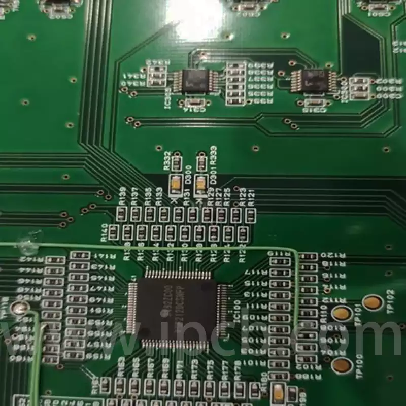
Printed Circuit Boards (PCBs) are fundamental in modern electronics, providing the necessary framework for connecting and supporting electronic components. Light Emitting Diodes (LEDs) are among the most widely used components in PCBs due to their efficiency, longevity, and versatility. A critical aspect of PCB design involving LEDs is the LED PCB footprint, which plays a crucial role in ensuring the component’s performance and reliability. This article delves into the intricacies of LED PCB footprints, covering design considerations, best practices, and common challenges.

What is an LED PCB Footprint?
An LED PCB footprint refers to the designated area on a PCB where an LED component is mounted. The footprint is integral to the PCB design as it dictates the placement, mechanical stability, and electrical connectivity of the LED. A well-designed footprint ensures that the LED is securely attached and functions as intended. Key features of an LED PCB footprint include:
- Pad Dimensions: Pads are areas on the PCB where the LED’s leads or pins are soldered. The dimensions of these pads must be precisely matched to the LED’s specifications to ensure a strong and reliable connection. Accurate pad dimensions prevent issues such as poor solder joints or mechanical instability.
- Solder Mask: The solder mask is a protective layer applied to the PCB to prevent solder from bridging between pads and other conductive areas. The footprint design must ensure that the solder mask openings align perfectly with the pad sizes to avoid soldering problems and ensure clean, accurate solder joints.
- Silkscreen Layer: This layer provides visual markers for component placement and orientation. The silkscreen layer includes labels and outlines that indicate the LED’s position and orientation on the PCB, aiding in correct placement during assembly.
- Thermal Management: High-power LEDs generate substantial heat, which can affect their performance and lifespan. Effective thermal management is crucial, and the footprint design should incorporate features such as thermal vias or larger copper areas to dissipate heat effectively and maintain optimal operating conditions for the LED.
Key Considerations for Designing an LED PCB Footprint
Designing an effective LED PCB footprint requires attention to several critical factors to ensure functionality and reliability:
- Component Specifications: Begin by consulting the LED manufacturer’s datasheet, which provides detailed specifications, including pad sizes, lead spacing, and overall dimensions. Accurate measurements are essential to ensure that the LED fits correctly and operates optimally.
- Pad Size and Shape: The dimensions and shape of the pads must match the LED’s leads to ensure proper soldering and mechanical support. The footprint should provide enough pad area for reliable solder joints while avoiding excessive space that could lead to solder bridges or weak connections. Pad shapes vary depending on the LED package, such as rectangular or circular pads.
- Clearance and Spacing: Adequate clearance around the LED footprint is necessary to prevent interference with adjacent components and facilitate proper soldering. Proper spacing minimizes the risk of mechanical damage and ensures ease of assembly. Ensure that the footprint design allows sufficient space between the LED and surrounding components.
- Thermal Management: For LEDs that generate significant heat, incorporating thermal management features into the footprint design is essential. This may involve adding thermal vias, heat sinks, or larger copper areas to improve heat dissipation and maintain the LED’s performance over time.
- Mounting Type: LEDs come in various mounting styles, including surface mount (SMD) and through-hole. The footprint design must correspond to the LED’s mounting type. Surface-mounted LEDs require pads on the PCB’s surface, while through-hole LEDs need drilled holes for their leads. Ensure that the footprint accommodates the LED’s mounting style.
- Manufacturing Tolerances: PCB manufacturing processes involve tolerances, and the footprint design should account for these variations. Including design margins to accommodate manufacturing tolerances helps ensure that the LED fits properly and functions as intended.
Best Practices for LED PCB Footprint Design
Adhering to best practices in LED PCB footprint design enhances the performance and reliability of the final product. Consider the following practices:
- Refer to Manufacturer’s Guidelines: Always consult the LED manufacturer’s datasheet for accurate and detailed footprint specifications. The datasheet provides critical information on pad sizes, lead spacing, and other dimensions necessary for precise design.
- Incorporate Thermal Management Features: For high-power LEDs, integrate thermal management solutions into the footprint design. This may include adding thermal vias, using heat sinks, or increasing copper areas to enhance heat dissipation and prevent overheating.
- Prototype Testing: Create prototypes to validate the accuracy and functionality of the LED footprint before finalizing the PCB design. Prototyping helps identify potential issues with component fit, soldering, or thermal performance, allowing for adjustments before mass production.
- Follow IPC Standards: Adhere to IPC (Institute for Printed Circuits) standards for PCB design. IPC standards provide established practices for component footprints, pad sizes, and clearances, ensuring compatibility and reliability in the final product.
- Automated Assembly Considerations: If the PCB will be assembled using automated pick-and-place machines, ensure that the LED footprint design accommodates the machine’s placement tolerances and capabilities. Adjust pad sizes or spacing as necessary to facilitate efficient automated assembly.
- Design for Manufacturability (DFM): Evaluate the footprint design for manufacturability to identify potential issues that could affect the PCB’s production. Check pad sizes, clearances, and alignment with manufacturing capabilities to ensure a smooth production process.
Common Challenges in LED PCB Footprint Design
Designing LED PCB footprints can present several challenges that need to be addressed to ensure a successful design:
- Alignment Issues: Misalignment between the LED and the PCB footprint can lead to poor soldering and unreliable connections. Ensure that the footprint design includes precise dimensions and alignment features to prevent such issues.
- Solder Bridging: Incorrect pad sizes or spacing can result in solder bridging, where solder creates unintended connections between pads. Proper pad layout and spacing are crucial to avoid solder bridging and ensure clean, reliable solder joints.
- Thermal Management: Inadequate thermal management can lead to overheating and reduced LED lifespan. Ensure that the footprint design incorporates sufficient thermal management features, especially for high-power LEDs, to maintain optimal operating conditions.
- Mechanical Stress: Mechanical stress during assembly or operation can damage the LED or its solder connections. Design the footprint with adequate clearance and support to minimize mechanical stress and prevent damage to the LED.
- Manufacturing Variations: Variations in PCB manufacturing processes can affect the accuracy of the LED footprint. Incorporate design margins to account for manufacturing tolerances and ensure a proper fit for the LED.
Advanced Considerations and Future Trends
As technology evolves, several emerging trends and advanced considerations are shaping LED PCB footprint design:
- Miniaturization: The trend toward smaller and more compact electronic devices requires miniaturized LED footprints. Designers must ensure that reduced footprint dimensions do not compromise performance or manufacturability.
- Flexible PCBs: The use of flexible PCBs is increasing, particularly in applications requiring curved or conformable surfaces. Designing LED footprints for flexible PCBs involves considerations such as flexibility, material compatibility, and mechanical stress.
- High-Brightness LEDs: High-brightness LEDs are used in applications that require intense light output. Designing footprints for these LEDs involves addressing higher thermal dissipation needs and ensuring robust mechanical support.
- Integrated Thermal Management Solutions: Advanced thermal management solutions, such as integrated heat spreaders and thermal interface materials, are becoming more common. Incorporating these solutions into the LED footprint design can enhance thermal performance and reliability.
- Environmental Considerations: There is a growing emphasis on environmental sustainability. Designers are exploring materials and processes that reduce environmental impact, including designing footprints for LEDs with lower energy consumption and using eco-friendly manufacturing techniques.
- Smart LEDs: The rise of smart LEDs with integrated sensors and communication capabilities introduces new design considerations. Footprints for smart LEDs must accommodate additional circuitry and components while maintaining compact dimensions.
- Modular Designs: Modular design approaches, where LEDs and other components are designed to be easily interchangeable or upgradeable, are gaining popularity. Designing footprints for modular LED systems involves ensuring compatibility with various module configurations and interfaces.
- Cost Efficiency: As technology advances, cost efficiency becomes increasingly important. Designers are focusing on optimizing LED footprint designs to balance performance, manufacturing cost, and component cost. This involves making trade-offs between complex features and cost-effective solutions while ensuring product quality and reliability.
- Enhanced Connectivity: With the rise of IoT (Internet of Things) and connected devices, there is a growing need for improved connectivity solutions in LED designs. This may include designing footprints that support additional communication interfaces or integrating LED control circuits within the footprint to accommodate modern connectivity requirements.
- Improved Reliability Testing: To ensure that LED footprints perform reliably under various conditions, designers are incorporating advanced reliability testing techniques. This includes subjecting prototypes to rigorous thermal cycling, mechanical stress, and long-term operation tests to identify potential failure modes and improve overall design robustness.
Conclusion
Designing an LED PCB footprint is a crucial aspect of PCB development that significantly impacts the performance, reliability, and manufacturability of electronic devices. By understanding the essential elements of LED PCB footprints, adhering to best practices, and addressing common challenges, designers can create effective and reliable PCB layouts for LED applications. Accurate footprint design, combined with thorough testing and adherence to industry standards, ensures that LEDs perform optimally and contribute to the overall success of the final product.
As technology advances and new trends emerge, staying informed about advanced considerations and integrating innovative solutions will further enhance LED PCB footprint design. By continually improving design practices and embracing emerging technologies, designers can meet the demands of modern electronic applications and deliver high-quality, reliable LED-based products.


