What is PCB? PCB is the core component of the electronic industry and the mother board of the electronic manufacturing industry. The development of PCB is closely linked to the rapid pace of electronic technology, jointly promoting the continuous innovation and progress of the electronic information industry. Due to its use of electronic printing, it is called a printed circuit board or Printed Wiring Board, PWB.
In 1936, PCBs were used in radios. In 1943, PCB technology was applied to military radios, and in 1948, PCBs became available for commercial use. Since the mid-1950s, PCBs have only been widely used.
Before the emergence of PCBs, the interconnection between electronic components relied on direct wire connections to form a complete circuit. At the beginning of the 20th century, in order to simplify the production of electronic machines, reduce wiring between electronic parts, and lower production costs, people began to explore the method of replacing wiring with printing.
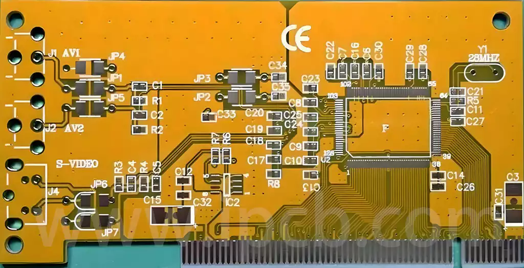
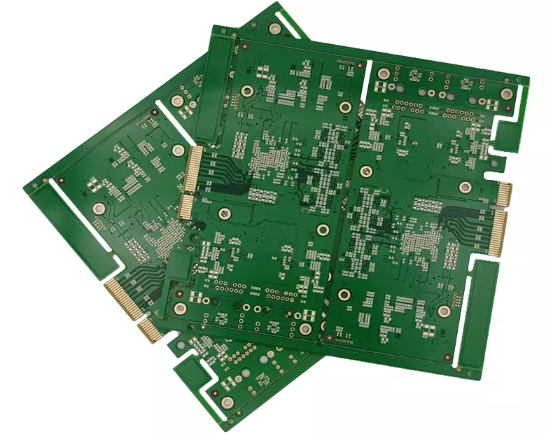
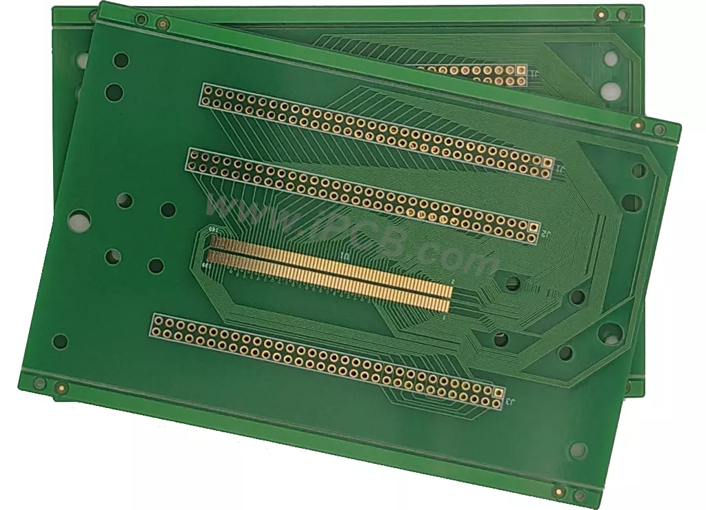
PCB includes rigid PCB, FPC, and rigid-flexible PCB. This also includes ceramic PCBs, alumina ceramic PCBs, aluminum nitride ceramic PCBs, circuit boards, PCB boards, aluminum substrates, high-frequency circuit boards, thick copper boards, impedance boards, PCB prototypes, ultra-thin circuit boards, ultra-thin PCBs, FR-4 PCBs, etc. PCB makes circuits more intuitive and plays an important role in mass production of fixed circuits and optimizing electrical layout.
According to the number of layers, PCBs are classified into three major categories: single-sided circuit boards, double-sided circuit boards, and multi-layer circuit boards.
Single-sided PCB is the most basic PCB, with parts concentrated on one side and wires concentrated on the other side. Because the wires only appear on one side, this type of PCB is called a single-sided circuit board. Single panel production is usually simple and cost-effective, but the disadvantage is that it cannot be applied to overly complex products.
Double-sided PCB is an extension of a single-sided circuit board. When single-layer wiring cannot meet the needs of electronic products, a double-sided circuit board needs to be used. Both sides are covered with copper and have wiring, and the wires between the two layers can be connected through vias to form the required network connection.
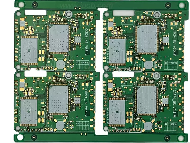
Multilayer PCB refers to a circuit board consisting of three or more layers of conductive graphics and insulating materials separated by layers, with conductive graphics interconnected as required. Multilayer circuit board is a product of the development of electronic information technology towards high speed, multifunctionality, large capacity, small volume, thinness, and lightweighting.
Classify by PCB Material
94HB ->94V0->22F ->CEM1->CEM3->FR4->High temperature substrate ->Metal substrate ->Ceramic substrate ->high speed substrate->High frequency substrate
The price of PCB
According to the design of the circuit board, the price will be determined based on the material of the circuit board, the number of layers of the PCB circuit board, the size of the PCB, the quantity produced each time, the production process, the minimum line width and spacing, the minimum aperture and number of holes, special processes, and other requirements There are several main ways to calculate prices in the PCB industry:
Calculate price based on size (applicable for small batches of samples)
PCB manufacturers will provide unit prices per square centimeter based on different layers and processes of the circuit board. Customers only need to change the size of the circuit board to centimeters and multiply it by the unit price per square centimeter to obtain the unit price of the circuit board to be produced. This calculation method is very suitable for ordinary process circuit boards, which is convenient for both PCB manufacturers and PCB buyers
For example, if a PCB manufacturer prices a single panel, FR-4 material, and an order of 10-20 square meters, with a unit price of 0.04 yuan/square centimeter, and the purchaser’s circuit board size is 10 * 10CM and the quantity produced is 1000-2000pcs, it exactly meets this standard, and the unit price is equal to 10 * 10 * 0.04=4 yuan/pcs
Calculate PCB prices based on cost refinement (applicable to large quantities)
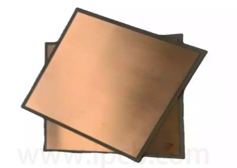
Because the raw material for PCB is copper-clad board, the factory that produces copper-clad board has set some fixed sizes for sale in the market, commonly 915mm * 1220mm (36 “* 48”); 940MM * 1245MM (37 “* 49”); 1020MM * 1220MM (40 “* 48”); 1067mm * 1220mm (42 “* 48”); 1042MM * 1245MM (41 “49”); 1093MM * 1245MM (43 “* 49”) PCB manufacturers will calculate the utilization rate of copper-clad boards for this batch of circuit boards based on the materials, layers, processes, quantities, and other parameters of the PCBs to be produced, thereby calculating the material cost
For example, it is necessary to produce a 100 * 100mm PCB, In order to improve production efficiency, the PCB factory may assemble 100 * 4 and 100 * 5 large boards for production. They also need to add some spacing and board edges for convenient production. Generally, the spacing between the gong boards is kept at 2MM, and the board edges are kept at 8-20MM. Then, the large boards formed are cut in the size of the raw materials. If they are cut exactly here, there are no extra boards, which is to maximize utilization. Calculating utilization is just one step, and drilling fees are also included to see how many holes there are, how big the smallest hole is, how many holes there are in a large board, and the cost of electroplating copper is calculated based on the wiring inside the board. Finally, the cost of each small process is added. The average labor cost, loss rate, profit margin, marketing expenses for each company, and finally dividing this total cost by how many small boards can be produced from a large piece of raw materials, Obtain the unit price of the small board. This process is very complex and requires a dedicated person to do it. Generally, quoting takes several hours or more.
PCB online quotation
Due to various factors affecting the price of circuit boards, ordinary PCB buyers are not familiar with the quotation process of PCB suppliers. It often takes a long time to obtain a price, wasting a lot of manpower and material resources. Additionally, in order to understand the price of a printed circuit board, individual contact information is handed over to the PCB factory, causing continuous sales harassment. Many PCB companies have started building a circuit board pricing program on their own websites, allowing customers to calculate prices freely through some rules. Even those who do not understand PCB can easily calculate PCB prices.
1 layer PCB process flow
Cutting and grinding ->Drilling ->Outer layer graphics ->(Full board gold plating) ->Etching ->Inspection ->Screen printing solder mask ->(Hot air leveling, HASL) ->Screen printing characters ->Appearance processing ->Testing ->Inspection
2 layer tin spray PCB process flow
Cutting and grinding ->Drilling ->Copper sinking and thickening ->Outer layer graphics ->Tin plating, etching and tin removal ->Secondary drilling ->Inspection ->Screen printing and solder resistance ->Gold plated plugs ->Hot air leveling ->Screen printing characters ->Appearance processing ->Testing ->Inspection
Process flow of 2-layer ENIG PCB
Cutting and grinding ->Drilling ->Copper sinking and thickening ->Outer layer graphics ->Nickel plating, gold film removal and etching ->Secondary drilling ->Inspection ->Screen printing resistance welding ->Screen printing characters ->Appearance processing ->Testing ->Inspection
Process flow of multi-layer tin sprayed PCB
Cutting and grinding ->drilling positioning holes ->inner layer graphics ->inner layer etching ->inspection ->blackening ->lamination ->drilling ->copper deposition and thickening ->outer layer graphics ->tin plating, etching and tin removal ->secondary drilling ->inspection ->silk screen solder mask ->gold-plated plugs ->hot air leveling ->silk screen characters ->external processing ->testing ->inspection
Process flow of multi-layer ENIG PCB
Cutting and grinding ->Drilling positioning holes ->Inner layer graphics ->Inner layer etching ->Inspection ->Blackening ->Lamination ->Drilling ->Copper deposition and thickening ->Outer layer graphics ->Gold plating and film removal etching ->Secondary drilling ->Inspection ->Screen printing resistance welding ->Screen printing characters ->Appearance processing ->Testing ->Inspection
Process flow of multi-layer deposited nickel gold PCB
Cutting and grinding ->drilling positioning holes ->inner layer graphics ->inner layer etching ->inspection ->blackening ->lamination ->drilling ->copper deposition and thickening ->outer layer graphics ->tin plating, etching and tin removal ->secondary drilling ->inspection ->silk screen solder mask ->chemical nickel gold deposition ->silk screen characters ->external processing ->testing ->inspection
As the most widely used electronic component product, PCB has strong vitality. Whether from the perspective of supply and demand or historical cycles, the sustained strong downstream demand has gradually driven the shipments of various PCB manufacturers in the PCB industry chain. The continuous development of PCB technology has made significant contributions to the advancement of human technology.