In the rapidly evolving world of electronics, custom PCB board printing has emerged as a vital process that facilitates the creation of highly specialized electronic devices. This process involves designing and fabricating printed circuit boards (PCBs) tailored to specific requirements, ensuring that they meet the unique needs of different applications. Whether in consumer electronics, medical devices, or industrial equipment, custom PCB board printing plays an essential role in the functionality and reliability of modern electronic systems.
Understanding PCBs
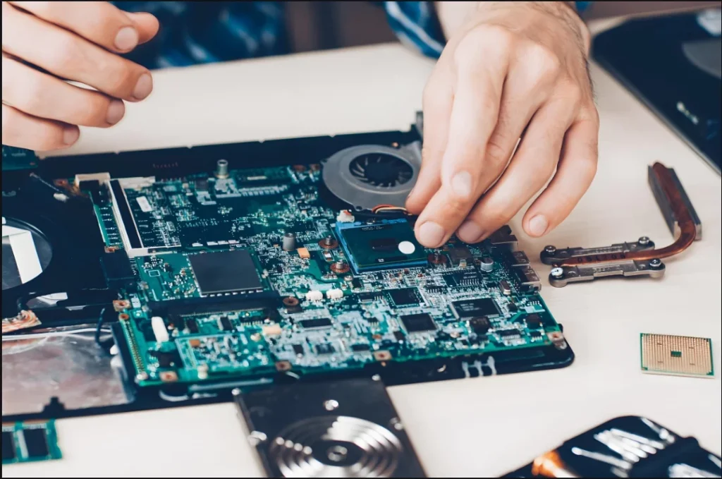
Before delving into the specifics of custom PCB board printing, it’s crucial to understand what a printed circuit board is. A PCB serves as the backbone of electronic devices, providing a platform for mounting components such as resistors, capacitors, and integrated circuits. Traditionally made from materials like fiberglass or epoxy resin, PCBs are designed to electrically connect these components through conductive pathways.
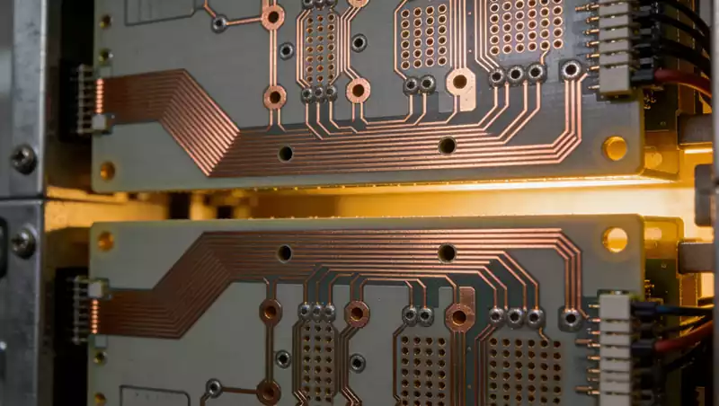
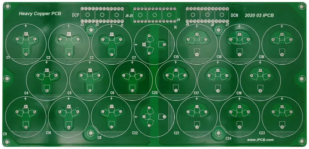
PCBs can vary significantly in terms of size, complexity, and the number of layers. Single-sided PCBs have components mounted on one side, while double-sided PCBs allow for components on both sides. More complex applications may require multi-layer boards, which can accommodate intricate designs and a higher density of components. The flexibility in design options allows engineers to innovate and optimize circuit layouts, leading to better performance in various applications.
The Importance of Customization
The demand for custom PCB board printing has grown due to the diverse requirements of modern electronics. Off-the-shelf PCBs may not meet the specific needs of every application, making customization essential. Custom PCBs enable manufacturers to optimize performance, reduce size, and enhance functionality, ultimately leading to more efficient electronic devices.
Customization is particularly important in industries such as medical technology, aerospace, and automotive, where precision and reliability are paramount. For example, a custom PCB used in a medical device must adhere to strict regulations and be designed to withstand various environmental factors. The ability to tailor the design ensures that the PCB meets these stringent requirements, minimizing the risk of failure in critical applications.
The Custom PCB Printing Process
Custom PCB board printing involves several steps, starting from initial design to final production. The following outlines the typical process involved:
- Designing the PCB: The process begins with the design phase, where engineers use specialized software to create a schematic representation of the PCB. This design outlines the layout, including the placement of components, trace routing, and the overall structure. Tools like Altium Designer, Eagle, or KiCad are commonly used for this purpose. In this phase, engineers must consider factors such as electrical performance, signal integrity, and thermal management.
- Creating the PCB Layout: After finalizing the schematic, the next step is to create a detailed PCB layout. This involves arranging the components on the board and routing the electrical connections. The layout must consider factors such as signal integrity, thermal management, and electromagnetic interference (EMI). A well-designed layout can prevent issues like crosstalk and ensure reliable operation of the electronic device.
- Printing the PCB: Once the design and layout are complete, the actual printing process begins. This typically involves a process called photolithography, where a light-sensitive material is applied to the surface of the PCB. A mask is then used to expose specific areas to UV light, creating a pattern that corresponds to the desired circuit design. This step is critical for defining the intricate patterns that will guide the electrical connections.
- Etching the PCB: After printing, the PCB undergoes an etching process to remove unwanted copper from the board. This leaves behind the conductive pathways that connect the various components. Etching can be done chemically or through laser techniques, depending on the desired precision and the complexity of the design. The choice of etching method can significantly impact the final quality of the PCB.
- Drilling Holes: The next step involves drilling holes for component leads and vias. Vias are essential for connecting different layers of a multi-layer PCB. The drilling process must be precise to ensure that components fit correctly and electrical connections are reliable. Accurate drilling is crucial for high-density designs where space is limited.
- Applying Solder Mask and Silkscreen: A solder mask is then applied to protect the copper traces from oxidation and short-circuiting. This mask also helps to prevent solder from bridging between adjacent pads during assembly. Additionally, a silkscreen layer is printed to provide labels and markings on the board for easier identification of components. This step enhances the usability of the PCB during assembly and maintenance.
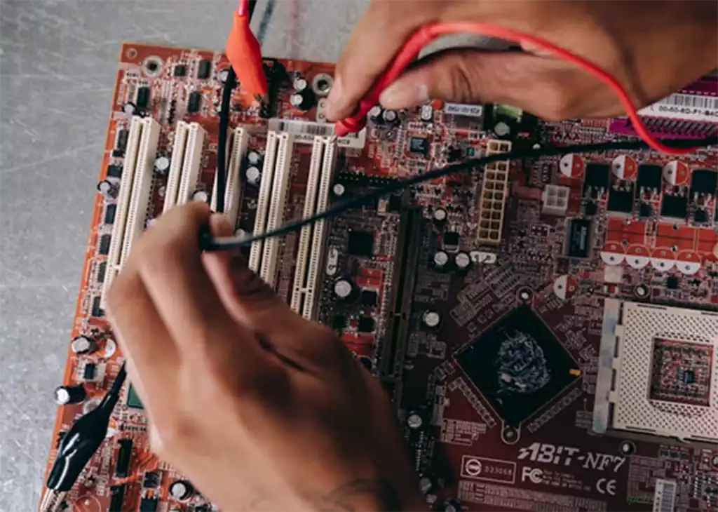
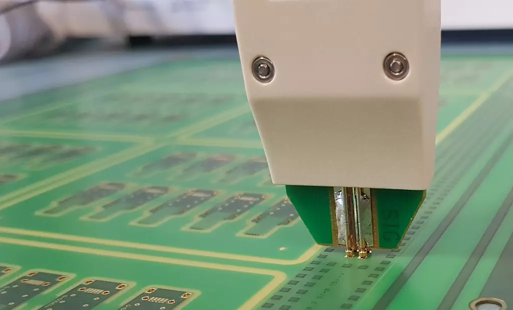
- Testing the PCB: Before the final product is ready, the custom PCB undergoes rigorous testing to ensure functionality and reliability. This may include visual inspections, electrical testing, and thermal analysis. Any defects found during testing can be addressed before mass production. Testing is vital to identify potential issues that could lead to product failures in the field.
- Assembly: Finally, the components are mounted onto the custom PCB, either through manual or automated processes. Surface mount technology (SMT) is commonly used for high-density applications, allowing for smaller components to be placed efficiently. The assembly process is critical for ensuring that the final product meets quality and performance standards.
Benefits of Custom PCB Board Printing
The advantages of custom PCB board printing are numerous, particularly for businesses seeking to innovate and differentiate their products in a competitive market:
- Tailored Solutions: Custom PCBs provide solutions tailored to specific applications, ensuring optimal performance and functionality. This level of customization allows companies to address unique challenges and meet customer demands effectively.
- Enhanced Performance: By optimizing the design of a PCB for a particular application, manufacturers can improve overall performance. Custom layouts can reduce signal loss, improve thermal management, and enhance power efficiency. This leads to more reliable and effective electronic devices.
- Cost Efficiency: While custom PCBs may require a higher initial investment, they often lead to long-term cost savings. Efficient designs can reduce material costs and minimize waste, while reliable PCBs reduce the risk of product failures and costly recalls. Companies can benefit from a better return on investment through fewer defects and improved product reliability.
- Shorter Time to Market: Custom PCB board printing enables faster prototyping and production, allowing companies to bring their products to market more quickly. This agility is essential in industries where technological advancements occur rapidly. Speeding up the design and manufacturing processes can provide a competitive edge.
- Support for Advanced Technologies: The trend towards miniaturization and increased functionality in electronic devices requires innovative PCB designs. Custom printing supports the integration of advanced technologies, such as IoT connectivity and smart components, into compact PCBs. This capability allows manufacturers to keep pace with evolving market demands.
Challenges in Custom PCB Board Printing
Despite the benefits, custom PCB board printing also presents several challenges:
- Complexity of Design: As designs become more complex, ensuring accuracy and reliability becomes increasingly difficult. Engineers must account for various factors, such as signal integrity and thermal management, which can complicate the design process. Balancing these considerations is crucial for a successful outcome.
- Higher Costs for Small Batches: Custom PCBs can be more expensive to produce in small quantities due to setup costs. Companies must weigh the benefits of customization against the financial implications, especially for low-volume applications. Finding the right balance between cost and quality is essential for success.
- Longer Lead Times: The customization process can extend lead times compared to off-the-shelf solutions. Manufacturers need to plan accordingly to meet production schedules and avoid delays in product launches. Effective project management can help mitigate these challenges.
Future Trends in Custom PCB Board Printing
The future of custom PCB board printing looks promising, driven by several emerging trends:
- Increased Automation: Automation in the PCB printing process is expected to rise, leading to higher precision and efficiency. Advanced manufacturing technologies will enable faster production times and lower costs. Automation can also reduce human error and improve overall quality.
- Integration of Flexible PCBs: The demand for flexible and rigid-flex PCBs is increasing, particularly in wearable technology and compact devices. Custom PCB board printing will play a crucial role in producing these innovative designs. Flexibility in PCB design allows for more versatile applications in various industries.
- Sustainability Initiatives: As the electronics industry moves towards more sustainable practices, custom PCB manufacturing will need to adopt environmentally friendly materials and processes. This shift will drive innovation in PCB design and production methods, promoting greener electronics.
- IoT and Smart Technology: The growth of IoT devices and smart technology will necessitate more complex and integrated PCB designs. Custom PCB board printing will be essential in developing these advanced solutions. Manufacturers must stay ahead of trends to remain competitive in the market.
- Advanced Materials: The exploration of new materials, such as biodegradable substrates and advanced conductive inks, will enhance the capabilities of custom PCBs. These materials can improve performance while reducing environmental impact. Research and development in materials science will drive future advancements.
Conclusion
Custom PCB board printing is a critical aspect of modern electronics, enabling manufacturers to create tailored solutions for a wide range of applications. By understanding the intricacies of the custom printing process, businesses can leverage these advantages to enhance performance, reduce costs, and innovate in an ever-changing market. As technology continues to evolve, custom PCB printing will play a central role in shaping the future of electronics, offering endless possibilities for innovation and advancement. The continuous pursuit of quality, efficiency, and sustainability will define the next generation of PCB manufacturing, paving the way for smarter, more connected devices.