In the entire process of SMT, precise printing of solder paste is the first step to achieve high-quality welding. To achieve this goal, a widely used and crucial tool is the solder paste stencil. The main function of this stencil is to print solder paste on demand onto the pads of the printed circuit board (PCB), laying a solid foundation for the subsequent component placement and welding process.

Basic composition and classification of stencils
In the manufacturing process of solder paste stencils, the choice of materials not only affects its strength, but also determines its durability and printing consistency. Different types of stainless steel have different tensile strengths and elastic moduli, which will directly affect the degree of deformation of the stencil in high-voltage printing. In addition, the surface treatment methods of stencils are becoming increasingly diverse, such as electropolishing, sandblasting, oxidation treatment, etc. These technologies help to improve the release behavior of solder paste.
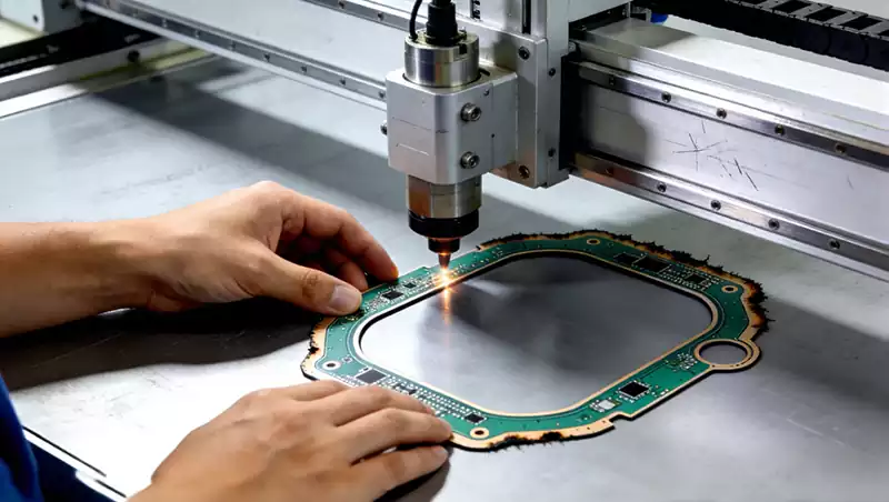
In terms of process selection, although the etched stencil is low-cost and suitable for mass production, its hole wall is rough and the size control is relatively poor. It is mainly suitable for products with low requirements for solder joint accuracy. Laser cutting steel mesh uses a high-power laser beam to precisely cut the material to form an opening with clear contours and precise dimensions. It is one of the most widely used template manufacturing technologies.
Considerations for template opening and layout
Reasonable template opening design should take into account the size of the pad, the structure of the component pins, the heat capacity of the solder joints and the reflow process parameters. For example, if too much solder paste is deposited under the thermal pad of high-power devices such as MOS tubes or large-size ICs, it is easy to cause problems such as floating solder and pad warping. Therefore, island-shaped or cross-shaped template openings are often used to balance the amount of solder paste while enhancing heat conduction.
Modern design tools such as Altium Designer and PADS support the automation of opening design, preset adaptive template parameters in the component package library, and improve engineering efficiency. At the same time, combined with 3D solder paste simulation software, the volume and distribution of solder paste can be estimated before actual printing, thereby reducing the cost of trial and error.
Control techniques for solder paste transfer efficiency
In terms of environmental control, the effects of humidity and temperature on the activity and fluidity of solder paste should not be ignored. It is usually recommended to perform solder paste printing in a workshop with a temperature of 23-27°C and a humidity of 40-60%. Too high a temperature may cause the solder paste to oxidize prematurely, while too low a temperature may affect its printing fluidity and form a “drawing” phenomenon.
In addition, the peeling speed between the steel mesh and the PCB will also significantly affect the integrity of the solder paste release. Ideally, the peeling should be slow and smooth to avoid the formation of residual glue or pulling off. Some high-end printing equipment even supports vacuum adsorption lamination to improve the printing alignment accuracy and transfer consistency.
Cleaning process and template life management
In terms of template cleaning, mainstream equipment usually has three methods of dry wiping, wet wiping and vacuum adsorption for coordinated use. Among them, wet wiping usually uses IPA or special cleaning fluid, with a brush and a scraper to clean the residual solder paste particles in the hole wall. For solder paste that has not been cleaned for a long time or has dried, ultrasonic cleaning is recommended.
In terms of life management, large manufacturing companies have incorporated templates into equipment asset management systems (such as ERP or MES), and regularly record information such as the number of uses, cleaning cycles, and abnormal alarms to ensure that each template is put into use in the best condition. Some factories also set a standard life limit (such as 5,000 times), and once it is reached, it will be forced to be replaced.
Adaptation and evolution with modern electronic packaging
With the rapid development of industries such as mobile terminals, wearable devices, and the Internet of Things, electronic components are evolving towards smaller sizes and higher integration, which poses unprecedented challenges to template technology. For example, 0.4mm or even 0.3mm pitch BGA packaging has become a regular requirement for high-end products. At such a small size, even slight template warping, excessive solder paste or offset may lead to serious problems such as bridging and cold soldering.
To adapt to this trend, in addition to using electroform stencils to meet the needs of ultra-fine pitch printing, the industry has also developed a structure called “Step Stencil”, which is to make thickness step designs in different areas on a template. This method allows high solder joints to maintain sufficient solder paste while keeping small solder joint areas under control, maximizing the compatibility of different package types.
In addition, some high-end customers will also require the template to print flux openings outside the pad to achieve better wettability and welding strength. With 3D SPI (solder paste thickness gauge) detection, more accurate data closed-loop control can be achieved.
Template manufacturing process and quality control
Every link in the template manufacturing process cannot be ignored. Especially in the laser cutting stage, parameters such as beam focal length, laser frequency, and moving speed directly determine the edge sharpness and aperture consistency of the opening. Generally speaking, laser equipment needs to be calibrated daily, and the cutting path must be strictly executed according to CAD data to avoid the “horse tooth edge” phenomenon.
Electropolishing is one of the key steps to improve the performance of the template. It uses chemical means to corrode the tiny burrs on the inner wall of the opening to make its surface smoother and reduce solder paste residue. In addition, high-quality steel mesh should also undergo stress release treatment to prevent the template from deforming due to temperature or tension changes during use.
In terms of final inspection, in addition to using traditional two-dimensional measuring instruments and microscopes, more and more companies are introducing 3D measurement systems to achieve comprehensive detection of opening depth, corner transition, and chamfering status. For key areas, the opening size deviation is even required to be controlled within ±3μm to ensure reliability under extreme processes.
Future trends: Nano coating and smart templates
The principle of nano coating is to form an extremely thin oleophobic and hydrophobic protective layer on the surface of the template, making it difficult for solder paste to adhere to the edge of the opening or the inner side of the hole wall, thereby improving the solder paste release efficiency and the durability of the template. The mainstream nano coatings on the market, such as NanoSlic and Alpha Tetra, have achieved the effect of reducing the solder paste residue rate by more than 30% and extending the cleaning cycle by more than 2 times to varying degrees.
At the same time, the concept of “smart template” is gradually moving from concept to implementation. Some large EMS manufacturers have begun to pilot the embedding of RFID tags or QR codes into the edge of the template. By scanning the code, information such as template model, production batch, cumulative printing times, cleaning records, etc. can be obtained, which greatly improves the traceability of use. Combined with the MES system, abnormal warning and data statistics can also be achieved to provide protection for preventing quality risks.
In addition, some template manufacturers are trying to embed strain gauges into the template body to monitor the template stress and deformation trend in real time during long-term use to prevent sudden breakage or warping. This “predictive maintenance” concept is gradually changing the passive strategy of “replace when broken” of traditional templates.
Practical application case analysis
In the production practice of another medical electronics customer, its ECG monitoring patch board uses a variety of 0201 and 0402 package components and adopts QFN-16 bottom heat dissipation package. Before mass production, the customer used traditional steel mesh for proofing, resulting in frequent problems of solder paste collapse and solder pad tin bias, which seriously affected the mounting accuracy and welding reliability.
Subsequently, the engineering team adopted the following improvement measures:
The local shrinkage hole design of the template, especially the 0201 area, controls the opening size within 0.18mm;
The hot pad adopts an island-type cross opening to ensure uniform heating of the solder paste;
The steel mesh adds nano-coating treatment to improve the efficiency of solder paste release;
The whole process introduces 3D SPI detection to establish a solder paste quality database.
In the end, the welding defect rate was reduced from 5.2% to 0.6%, greatly improving production efficiency and customer satisfaction. This case once again proves that although the template is small, it is a big entrance to quality control.
Analysis of the correlation between welding defects and templates
In the production site, welding defects are often the result of the interaction of multiple factors. And the template is one of the key factors affecting this process. For example:
Bridging: Common in fine-pitch QFP or BGA devices, mainly caused by too wide template opening, excessive solder paste coating, printing offset, etc.;
Open: May be caused by steel mesh blocking holes, insufficient opening design, or inconsistent stripping speed between steel mesh and PCB;
Insufficient solder: Mostly related to too small Area Ratio and unreasonable template thickness design, especially common in hot pads or bottom solder joints.
In order to systematically analyze the causal relationship between templates and welding defects, some advanced factories have developed a defect tracing model, which binds each PCB printing image with the template opening data to form a traceable solder joint database, and combines machine learning technology to classify defect patterns to provide a basis for continuous improvement.
Application expansion of templates in special processes
In addition to conventional SMT printing processes, templates also play an irreplaceable role in many special processes:
Red glue template: designed for double-sided mounting, its printed red glue is used to fix components, the template opening is larger and the layout is more dispersed;
Solder paste printing template: used in selective wave soldering to improve the consistency of wave soldering;
High-frequency board template: on high-frequency PCB (such as PTFE, ceramic substrate), due to the different surface energy and adhesion, the template opening and scraper contact angle need to be specially designed.
In the future, with the development of flexible electronics and printed electronics technology, the design of templates will also transcend the traditional 2D form and develop towards 3D deformation templates, adjustable templates, etc.
Conclusion
In the entire SMT process chain, the template seems to be just a consumable tool, but it actually contains many core technologies such as precision processing, process control, data traceability and intelligent manufacturing. From material selection to design, from manufacturing to application, and then to the future intelligent evolution, it is not just a “printing medium”, but also a microcosm of process accuracy and a threshold for quality control.
Today, lean manufacturing and high reliability are constantly emphasized. Whoever has the ability to manage high-quality templates will gain an advantage in electronic manufacturing. In the future, as the construction of intelligent factories is further promoted, the role of templates will become more and more important, becoming a bridge to promote the deep integration of Industry 4.0 and electronic manufacturing.