In the ever-evolving world of electronics, the demand for smaller, more powerful, and more efficient devices is constantly growing. At the heart of these advancements is the HDI multilayer PCB (High-Density Interconnect multilayer printed circuit board), a technology that has revolutionized how electronic circuits are designed and manufactured. This type of PCB is crucial in modern electronics, providing the foundation for the miniaturization of devices while maintaining high performance and reliability.
What is an HDI Multilayer PCB?
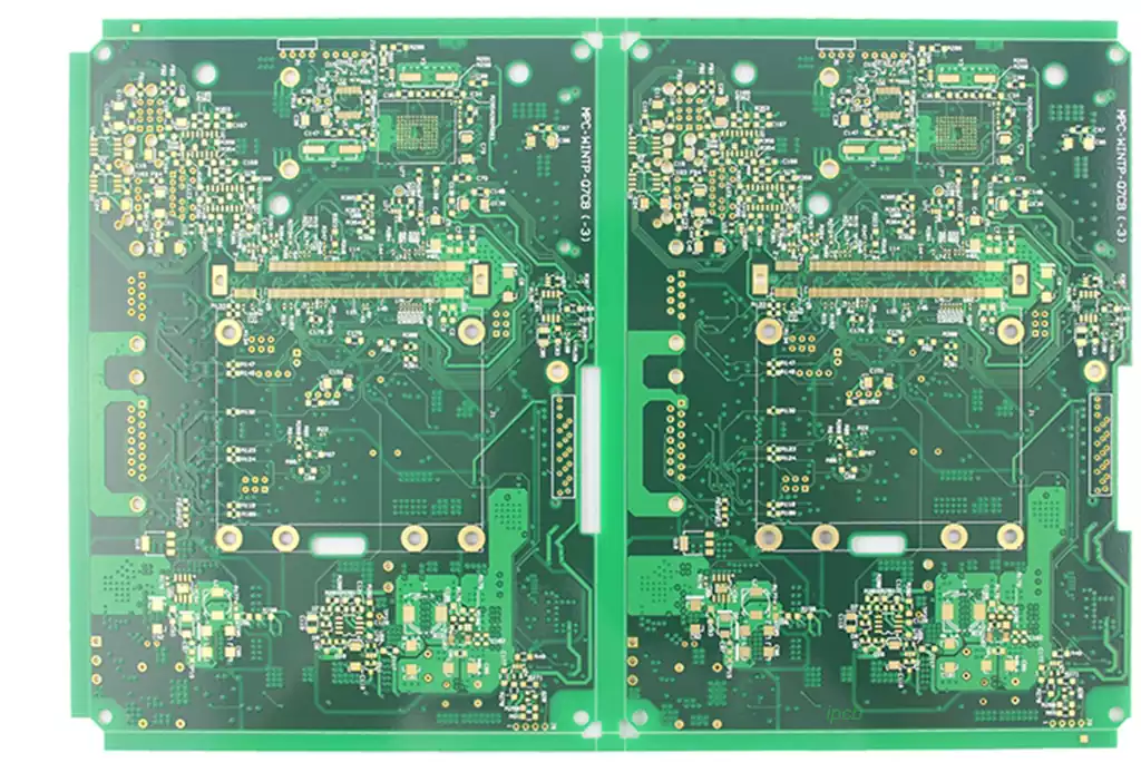
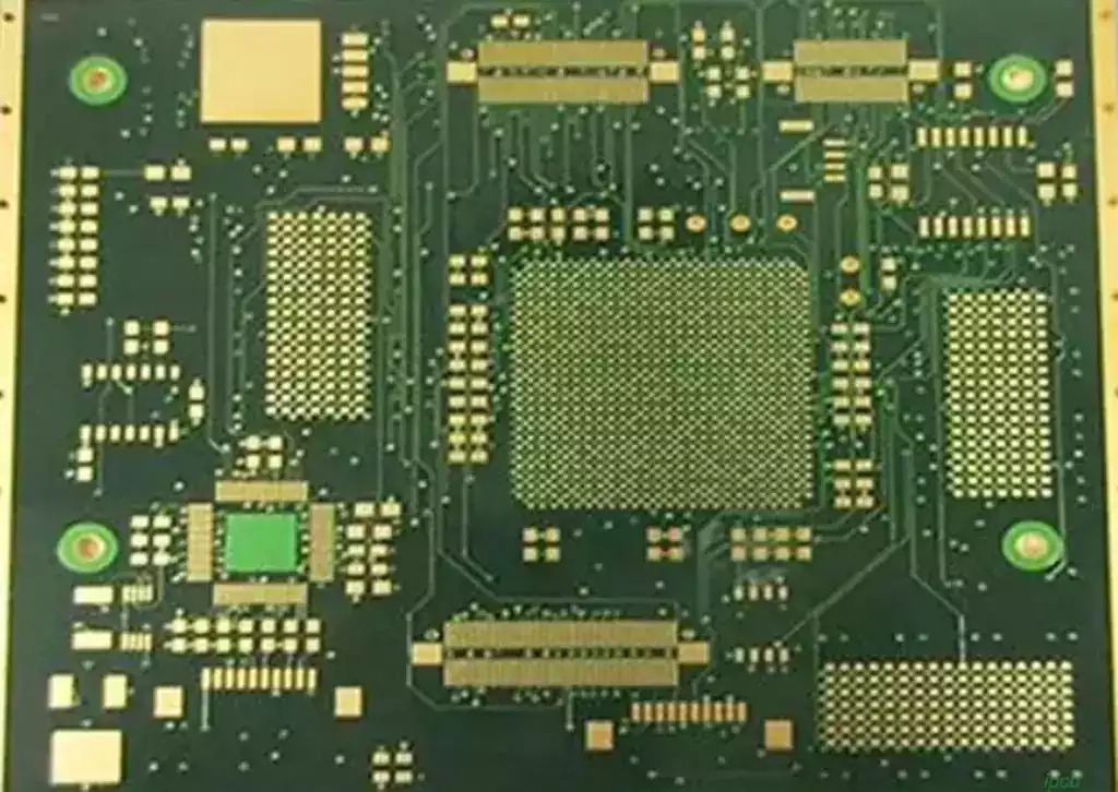
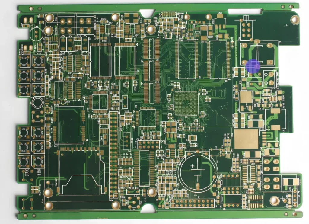
An HDI multilayer PCB is a type of printed circuit board that features a higher wiring density per unit area compared to traditional PCBs. This is achieved by incorporating more layers and utilizing microvias, blind vias, and buried vias. These features allow for more compact designs, enabling the development of smaller, more efficient electronic devices. The technology allows components to be placed closer together, reducing the overall size of the board without sacrificing functionality.
Key Features of HDI Multilayer PCBs
Increased Layer Count
HDI multilayer PCBs are characterized by their increased layer count. Traditional PCBs might have only a few layers, but an HDI multilayer PCB can have as many as 20 or more. These additional layers provide more space for routing signals and power, which is essential for complex electronic devices that require high performance and reliability. The ability to stack multiple layers within a compact space is one of the primary advantages of HDI technology.
Use of Microvias, Blind Vias, and Buried Vias
One of the most significant innovations in HDI multilayer PCB design is the use of microvias, blind vias, and buried vias. Microvias are extremely small holes that connect different layers of the PCB, allowing for more complex routing without taking up much space. Blind vias connect an outer layer to one or more inner layers but do not go through the entire board, while buried vias connect inner layers without reaching the outer layers. These types of vias are essential for reducing the overall size of the PCB and increasing the density of components.
Enhanced Signal Integrity
The shorter signal paths in HDI multilayer PCB designs result in enhanced signal integrity. In high-speed circuits, maintaining signal integrity is crucial to prevent data loss and ensure reliable operation. HDI technology helps reduce signal interference and crosstalk, which can be problematic in densely packed boards. This feature is particularly important in applications where high-speed data transmission is required, such as in telecommunications and computing devices.
Improved Power Distribution
HDI multilayer PCBs also offer improved power distribution. The use of multiple layers allows for the creation of separate planes for power and ground, which helps in managing power delivery more efficiently. Proper power distribution is critical for ensuring that all components on the PCB receive stable and reliable power, which is essential for the overall performance of the device. This feature is particularly beneficial in high-power applications where power integrity is a major concern.
Advantages of HDI Multilayer PCBs
Miniaturization of Electronic Devices
One of the most significant advantages of HDI multilayer PCBs is their contribution to the miniaturization of electronic devices. As consumer demand shifts toward smaller, more portable devices, manufacturers face the challenge of fitting more functionality into less space. HDI multilayer PCB technology allows for the design of compact boards that can accommodate a high density of components, enabling the production of smaller devices without compromising performance.
Higher Component Density
The ability to support higher component density is another advantage of HDI multilayer PCB technology. By utilizing microvias, blind vias, and buried vias, designers can place components closer together and increase the overall density of the board. This is particularly important in applications that require complex circuitry, such as smartphones, tablets, and wearable devices. The higher component density not only improves the functionality of the device but also contributes to its overall compactness.
Improved Performance and Reliability
HDI multilayer PCBs are known for their improved performance and reliability. The shorter interconnects and enhanced signal integrity reduce the chances of signal degradation and data loss, which are common issues in high-speed circuits. Additionally, the precise manufacturing processes used in HDI technology result in fewer defects and higher overall reliability. This makes HDI multilayer PCBs suitable for use in mission-critical applications, where performance and reliability are paramount.
Cost-Effectiveness in High-Volume Production
While the initial cost of designing and manufacturing HDI multilayer PCBs may be higher compared to traditional PCBs, they become cost-effective in high-volume production. The ability to integrate more functionality into a single board reduces the need for additional components and interconnects, lowering the overall production cost. Additionally, the miniaturization achieved through HDI technology can lead to savings in materials and assembly time, further contributing to cost-effectiveness.
Design Flexibility
HDI multilayer PCBs offer a high degree of design flexibility. The use of multiple layers, microvias, and advanced routing techniques allows designers to create innovative and efficient layouts that meet the specific requirements of their applications. This flexibility is particularly valuable in industries where space constraints are a significant concern, such as in the design of mobile devices, medical equipment, and aerospace technology.
Applications of HDI Multilayer PCBs
Consumer Electronics
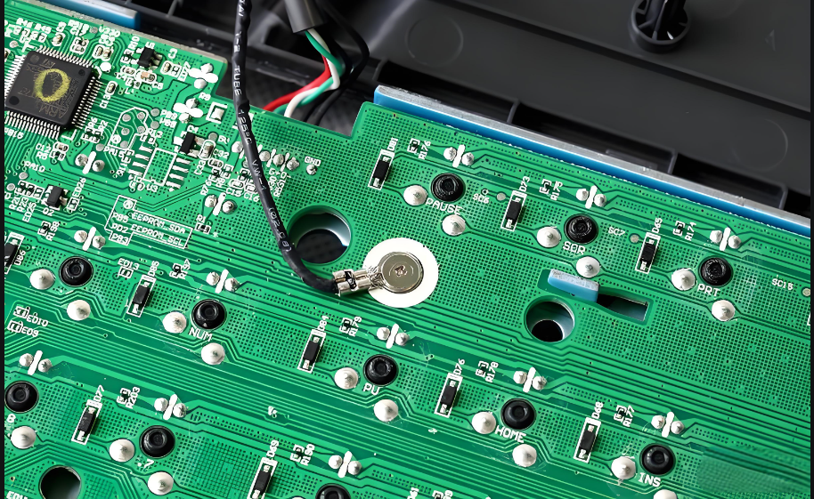
In the consumer electronics industry, HDI multilayer PCBs are widely used in the production of smartphones, tablets, laptops, and other portable devices. These devices require compact, high-performance PCBs that can support a large number of components within a small footprint. HDI technology enables the production of thinner, lighter devices with enhanced functionality, meeting the demands of modern consumers for portable and powerful electronic devices.
Automotive Industry
The automotive industry has seen a significant increase in the use of HDI multilayer PCBs in recent years. These PCBs are used in advanced driver-assistance systems (ADAS), infotainment systems, and various electronic control units (ECUs) within vehicles. HDI technology provides the high performance, reliability, and compactness needed for these critical automotive applications, ensuring that vehicles operate safely and efficiently.
Medical Devices
The medical industry is another area where HDI multilayer PCBs play a crucial role. As medical devices become more sophisticated and compact, the need for high-density, reliable PCBs has grown. HDI technology enables the development of complex medical devices, such as pacemakers, diagnostic equipment, and wearable health monitors, that require precise and reliable performance in a small form factor.
Aerospace and Defense
In the aerospace and defense industries, the reliability and performance of electronic systems are of utmost importance. HDI multilayer PCBs are used in avionics, communication systems, radar equipment, and other critical applications where size, weight, and performance are key considerations. The ability of HDI technology to meet the stringent requirements of these industries makes it an ideal choice for aerospace and defense applications.
Telecommunications
The telecommunications industry relies heavily on HDI multilayer PCBs to support the growing demand for high-speed data transmission and the expansion of 5G networks. HDI technology allows for the creation of PCBs that can handle the high frequencies and data rates required for modern telecommunications equipment. This includes everything from base stations to mobile devices, ensuring that the telecommunications infrastructure remains robust and capable of supporting the increasing data demands.
Challenges in Manufacturing HDI Multilayer PCBs
Complex Design and Manufacturing Processes
The design and manufacturing processes for HDI multilayer PCBs are more complex than those for traditional PCBs. The use of microvias, blind vias, and buried vias requires advanced fabrication techniques and precise control over the manufacturing process. Additionally, designers must carefully consider factors such as signal integrity, thermal management, and mechanical stability, which add to the complexity of the design process. These challenges can result in longer development times and higher costs, particularly for low-volume production.
Higher Production Costs
While HDI multilayer PCBs offer numerous advantages, they can be more expensive to produce, especially in low-volume runs. The advanced materials, processes, and equipment required for HDI manufacturing contribute to these higher costs. However, these costs can be offset in high-volume production, where the benefits of miniaturization and integration become more pronounced, making HDI PCBs a cost-effective solution for large-scale manufacturing.
Reliability Concerns
Although HDI multilayer PCBs are generally reliable, the increased complexity of these boards can introduce potential failure points. For example, the use of microvias can lead to issues such as via fatigue or delamination if not properly designed and manufactured. To mitigate these risks, it is essential to work with experienced PCB manufacturers who have a proven track record in HDI technology. Ensuring that the design and manufacturing processes are meticulously controlled is crucial for maintaining the reliability of HDI multilayer PCBs.
The Future of HDI Multilayer PCBs
The future of HDI multilayer PCBs looks promising, with continued advancements in technology driving their adoption across various industries. As the demand for smaller, more powerful, and more efficient electronic devices grows, HDI technology will play a critical role in meeting these needs. The ongoing development of 5G technology, the Internet of Things (IoT), and artificial intelligence will further increase the demand for high-performance PCBs, solidifying the importance of HDI multilayer PCBs in the electronics industry.
Conclusion
HDI multilayer PCBs represent a significant advancement in PCB technology, offering numerous benefits, including miniaturization, higher component density, improved performance, and cost-effectiveness in high-volume production. Despite the challenges associated with their design and manufacturing, the advantages of HDI multilayer PCBs make them indispensable in the development of modern electronic devices. As technology continues to evolve, the role of HDI multilayer PCBs in the electronics industry will only become more critical, paving the way for the next generation of innovative and efficient electronic products.