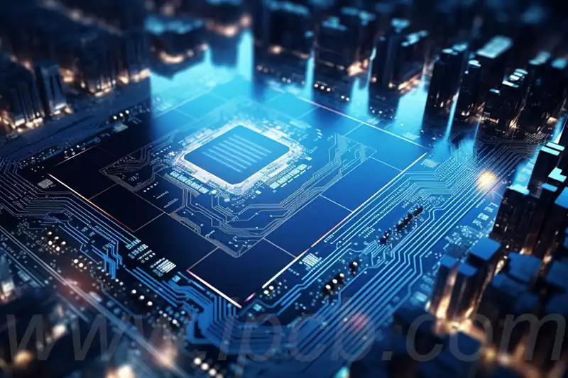
In the world of electronics and manufacturing, abbreviations are often used to streamline communication and enhance efficiency. What does the abbreviation PWB Stand For? One such abbreviation, “PWB,” is commonly encountered, especially in industries related to electronic devices, circuit boards, and assembly processes. While many people are familiar with the term PCB, or Printed Circuit Board, fewer may know what PWB stands for. This article will explore the meaning of PWB, its historical context, and its significance in today’s electronics manufacturing landscape.
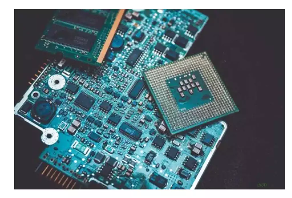
What Does PWB Stand For?It refers to a basic platform used to mechanically support and electrically connect electronic components using conductive pathways, or traces, etched from copper sheets laminated onto a non-conductive substrate. These pathways form the foundation of an electronic circuit, allowing electrical current to flow and components to function correctly. The abbreviation PWB was widely used in earlier stages of electronics manufacturing before the term PCB became prevalent.
Evolution from PWB to PCB
The terms PWB and PCB may seem interchangeable, but there is a notable evolution in the meanings. Initially, PWB referred specifically to the board that contained only the conductive traces or wiring patterns without any components mounted on it. In other words, a PWB was just the physical substrate that provided the layout for electrical connections.
However, as technology advanced, the boards became more complex, and engineers started integrating components directly onto the board. This development led to the Printed Circuit Board (PCB), which not only had the wiring but also included the various electronic components like resistors, capacitors, and microchips. This innovation reduced the need for manual wiring and made electronic circuits more compact, reliable, and cost-effective. Thus, PCB became the more common term, although PWB still describes the initial stages of board fabrication.
Differences Between PWB and PCB
The distinction between PWB and PCB may seem minor, but in specific technical contexts, it carries significant implications. Let’s dive deeper into the differences and explore how each term is used in electronics manufacturing and assembly.
1. PWB as a Subset of PCB
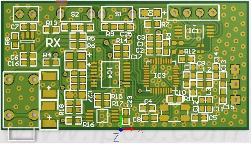
In many ways, PWB is a subset of PCB. A Printed Wiring Board is essentially the “skeleton” or foundation of a circuit, consisting of a non-conductive board (often made of fiberglass or another insulating material) with conductive wiring patterns on its surface. These patterns are created through various techniques such as etching, printing, or plating to establish electrical pathways.
A PWB on its own does not include electronic components. It merely provides the infrastructure for potential connections. Once components like transistors, capacitors, and integrated circuits are mounted onto the PWB, it becomes a Printed Circuit Board (PCB). In short, every PCB begins as a PWB, but not all PWBs evolve into PCBs.
2. PWB Focuses on Wiring, PCB on Functionality
The key difference lies in the functionality each term represents. A PWB focuses solely on the wiring layout—the conductive traces that will carry signals between different points on the board. These traces are the board’s “roads,” guiding electrical signals across the circuit.
On the other hand, a Printed Circuit Board is a fully functional unit that not only includes these wiring patterns but also the various components that complete the circuit. In other words, while a PWB is focused on the wiring itself, a PCB represents the completed electronic system, ready to be connected and used in a device.
3. Component Placement: The Shift from PWB to PCB
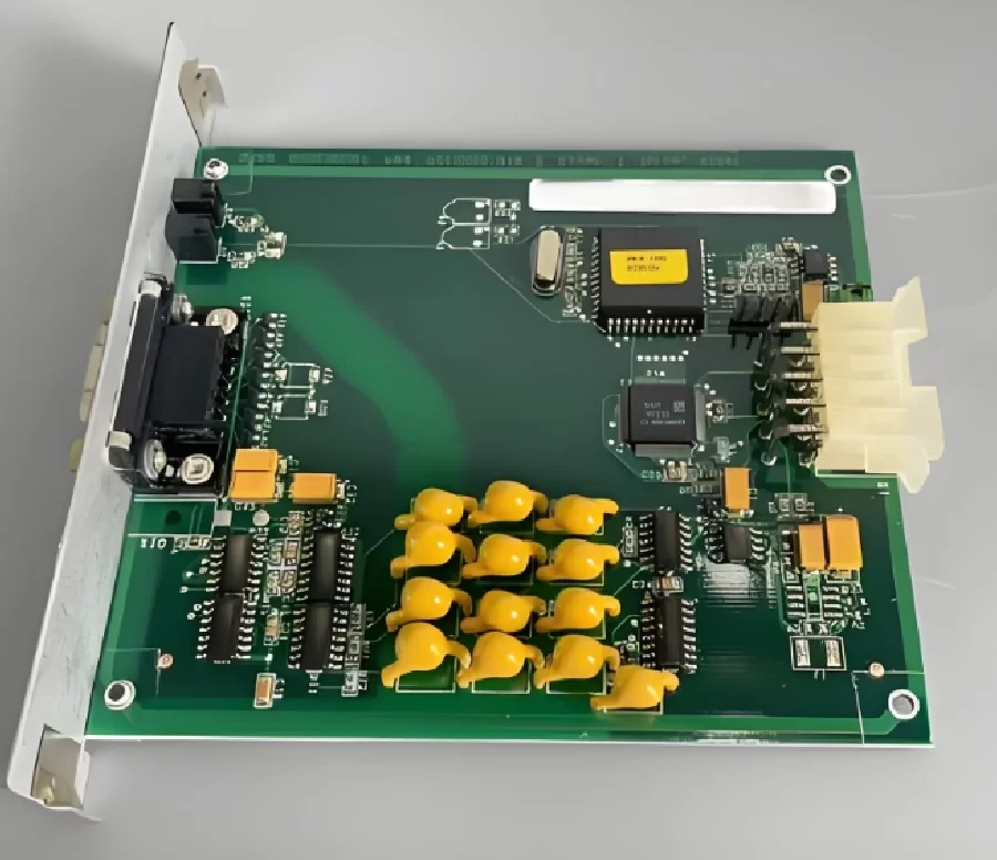
The transition from a Printed Wiring Board to a Printed Circuit Board occurs when components are added to the board. In this phase, various elements such as diodes, resistors, ICs, and connectors are soldered onto the PWB. After this, it’s no longer just a wiring board—it becomes a full-fledged circuit board capable of performing specific functions in electronic devices.
4. Historical Use of the Terms
In the earlier stages of electronics manufacturing, the term PWB was more commonly used, particularly in simpler circuits where the board was mainly a platform for holding external components. As the complexity of circuits grew, the need for integrating components directly onto the board became more apparent. The term PCB, therefore, gained traction as engineers developed methods for attaching components and creating fully assembled boards.
Even though PCB has become the dominant term, especially in contemporary electronics, PWB is still used in certain industries or contexts, particularly when emphasizing the board before component assembly. In technical documents and manufacturing specifications, the distinction between PWB and PCB may still be relevant when discussing the fabrication process.
5. Modern Usage and Confusion
In modern electronics, the two terms are often used interchangeably, leading to some confusion. Most engineers, designers, and manufacturers today prefer the term PCB, as it captures the full functionality of the board. However, some still use PWB, particularly when referring to the blank board before the components are mounted. This use is more common in the initial design, prototyping, or fabrication stages, where the emphasis is on the wiring patterns rather than the completed assembly.
Applications of PWBs and PCBs
Both PWBs and PCBs are critical in a wide variety of industries. While their functionality might differ, they are essential components in modern electronic devices and systems.
- Consumer Electronics: PWBs and PCBs are fundamental in products like smartphones, televisions, gaming consoles, and laptops. The circuit boards are the backbone of these devices, connecting all the necessary components.
- Automotive Systems: In modern vehicles, PCBs are used to control everything from engine management systems to entertainment and navigation features. PWBs serve as the foundational structure upon which these PCBs are built.
- Medical Devices: PWBs and PCBs are also crucial in medical technology, providing the necessary structure and connections for devices like heart monitors, MRI machines, and diagnostic tools. The precision and reliability of these boards are paramount in ensuring accurate medical diagnostics and treatments.
- Aerospace and Defense: In high-performance applications such as aerospace and defense, PWBs and PCBs need to meet stringent reliability standards. These boards must withstand extreme conditions such as high temperatures, vibrations, and shocks.
- Industrial Applications: In industrial equipment, PWBs and PCBs control systems such as automation processes, power management, and robotic systems. These boards enable precise control over machinery, helping industries achieve greater efficiency and reliability.
PWB and PCB Reliability Considerations
When it comes to designing and manufacturing Printed Wiring Boards (PWB) and Printed Circuit Boards (PCB), reliability is a critical factor, especially in industries where equipment failure can lead to significant consequences, such as in aerospace, medical devices, and automotive systems. The durability and performance of these boards are largely dependent on the quality of materials, manufacturing processes, and design precision.
In terms of material selection, PWBs and PCBs can be constructed using various substrates, with FR4 being one of the most common due to its affordability and excellent electrical insulation properties. However, high-performance applications may require specialized materials like polyimide for flexibility or ceramics for extreme temperature resistance. These materials must not only support the required circuitry but also ensure that the board can withstand environmental stressors like vibration, humidity, and thermal cycling.
Moreover, manufacturing processes play a crucial role in the final quality of a PWB or PCB. Techniques such as multi-layer construction, surface-mount technology (SMT), and through-hole plating allow boards to support increasingly complex electronic systems. Ensuring that these processes are carried out with precision is key to avoiding defects such as delamination, shorts, and open circuits, which can compromise board functionality.
As electronic devices become more integrated into critical applications, the importance of reliable and robust PWBs and PCBs cannot be overstated. Testing and validation processes, such as thermal cycling, vibration testing, and impedance measurement, are essential to ensure that the final product will perform consistently under varying conditions. By addressing potential reliability concerns in the design and manufacturing stages, companies can avoid costly repairs and ensure that their products meet industry standards for quality and safety.
This focus on reliability further highlights the distinction between the PWB, which is the initial stage of the process, and the final PCB, which needs to meet stringent performance requirements before it can be deployed in real-world applications.
The Future of PWB and PCB Technology
As technology evolves, so does the role of PWBs and PCBs in electronics. Several key trends are driving the future of these essential components:
- Miniaturization: As devices become smaller and more compact, the need for advanced PWB and PCB designs grows. Modern circuit boards must be able to support increasingly dense wiring patterns and accommodate tiny components without sacrificing performance.
- Flexible and Rigid-Flex Boards: Flexible PWBs are becoming more common, especially in applications where traditional rigid boards are impractical. Wearable technology, for example, requires flexible boards that can bend and conform to the shape of the body or clothing. This trend is driving new innovations in materials and manufacturing processes.
- Environmental Concerns: With growing environmental awareness, manufacturers are seeking ways to produce PWBs and PCBs that are more environmentally friendly. Lead-free soldering, recyclable materials, and energy-efficient manufacturing processes are just a few of the ways the industry is adapting to reduce its environmental footprint.
- 3D Printed Circuit Boards: Another exciting development is the rise of 3D-printed PWBs and PCBs. This technology allows for faster prototyping, reduced costs, and greater design flexibility. 3D printing has the potential to revolutionize the way circuit boards are manufactured, particularly in custom or low-volume applications.
Conclusion
To conclude, PWB, or Printed Wiring Board, refers to a crucial part of the electronics industry that forms the foundation for complex circuits. Though often overshadowed by the term PCB, the significance of the PWB in the design and manufacturing process remains essential. Understanding the difference between PWB and PCB can enhance one’s comprehension of electronics and the stages involved in creating the intricate devices we rely on daily.
The evolution from PWBs to PCBs highlights how electronics manufacturing has advanced, shifting from simple wiring platforms to fully integrated circuits capable of handling increasingly complex tasks. As technological trends like miniaturization, flexible boards, and 3D printing emerge, PWBs and PCBs will continue to adapt, playing a central role in the future of electronics.