What is pcba manufacturing? It is a critical process in the production of electronic devices. It involves the assembly of electronic components onto a printed circuit board (PCB) to create functional electronic circuits. This process is intricate, requiring precision, attention to detail, and adherence to quality standards to ensure the reliability and performance of the final product. This article explores the various stages and aspects of PCBA manufacturing, providing a comprehensive overview of the subject.
The Basics of PCBA Manufacturing
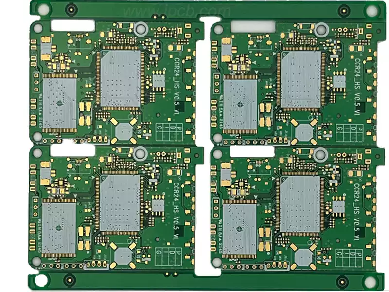
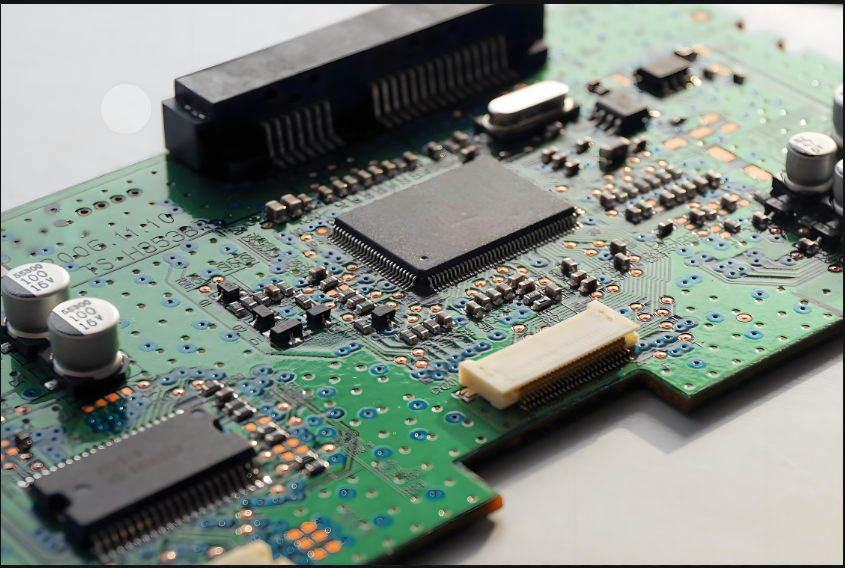
PCBA manufacturing is a multi-step process that starts with the design and production of the PCB, followed by the mounting and soldering of components, and finally, testing and quality control. Each stage is crucial in ensuring that the final product meets the required specifications and performance standards.
PCB Design and Fabrication
The journey of PCBA manufacturing begins with the design of the PCB. This involves creating a schematic diagram that outlines the connections and components needed for the circuit. Engineers use computer-aided design (CAD) software to develop the layout, considering factors like signal integrity, power distribution, and component placement.
Once the design is finalized, the PCB fabrication process begins. This involves the creation of the physical board, which typically consists of multiple layers of conductive material separated by insulating layers. The fabrication process includes several steps:
- Substrate Preparation: The base material, usually made of fiberglass, is coated with a thin layer of copper on both sides. This copper layer serves as the foundation for creating the circuit pattern.
- Patterning: A photosensitive film is applied to the copper layer, and ultraviolet light is used to transfer the circuit pattern onto the film. The film acts as a stencil, allowing precise areas of copper to be exposed or protected.
- Etching: The exposed copper is etched away using a chemical solution, leaving behind the desired circuit pattern. This step is crucial as it defines the electrical pathways on the PCB.
- Drilling: Holes are drilled into the board to create vias, which allow for electrical connections between different layers. These holes are essential for multi-layer PCBs where inter-layer connectivity is required.
- Plating: The holes are plated with copper to establish electrical continuity. This plating process also reinforces the structural integrity of the vias.
- Solder Mask Application: A protective solder mask is applied to prevent solder from bridging between conductors during assembly. The solder mask also protects the copper traces from oxidation and damage.
- Silkscreen Printing: Component labels and other markings are printed on the board for reference during assembly. These markings aid in identifying the correct placement and orientation of components.
Component Procurement
After the PCB is fabricated, the next step is procuring the necessary components. These components include resistors, capacitors, integrated circuits, connectors, and other electronic parts. Sourcing high-quality components is vital to ensure the reliability of the final product. Manufacturers often work with reputable suppliers and may use automated systems to manage inventory and track component availability.
Component procurement involves several key considerations:
- Component Specifications: Each component must meet specific electrical and mechanical requirements outlined in the design. Engineers specify parameters such as resistance, capacitance, tolerance, and power ratings.
- Supplier Selection: Choosing reliable suppliers is crucial for ensuring the quality and consistency of components. Manufacturers often establish long-term relationships with trusted suppliers.
- Inventory Management: Efficient inventory management systems help track component stock levels, forecast demand, and minimize lead times. This ensures that production schedules are met without delays.
- Component Testing: Incoming components are often subjected to quality control tests to verify their performance and compliance with specifications. This step helps prevent defective components from entering the assembly process.
Surface Mount Technology (SMT) Assembly
The majority of modern PCBAs are produced using Surface Mount Technology (SMT), which involves mounting components directly onto the surface of the PCB. SMT has largely replaced the older Through-Hole Technology (THT) due to its advantages in terms of space-saving, performance, and manufacturing efficiency. The SMT assembly process consists of several steps:
- Solder Paste Application: A stencil is used to apply solder paste to the pads on the PCB where components will be mounted. The solder paste consists of tiny solder particles suspended in a flux medium, which aids in the soldering process.
- Component Placement: Automated pick-and-place machines accurately position the components onto the solder paste-covered pads. These machines use vision systems to ensure precise placement and orientation of components.
- Reflow Soldering: The board is passed through a reflow oven, where the solder paste melts and forms solder joints, securing the components in place. The reflow oven heats the board in a controlled manner, allowing the solder to flow and solidify, creating reliable electrical connections.
SMT assembly offers several advantages:
- Miniaturization: SMT allows for the placement of smaller components, enabling the production of compact and lightweight devices.
- High-Density Assembly: Components can be placed on both sides of the PCB, maximizing the use of available space and enabling complex circuit designs.
- Automation: The use of automated machines in SMT assembly increases production speed and reduces the risk of human error, resulting in higher manufacturing efficiency.
Through-Hole Technology (THT) Assembly
While SMT is the predominant method for assembling PCBs, THT is still used for specific applications, particularly when components need to withstand mechanical stress or when high-power components are involved. In THT, components have leads that are inserted into holes drilled in the PCB and soldered on the opposite side. The THT assembly process includes:
- Component Insertion: Components are manually or automatically inserted into the drilled holes on the PCB. The leads protrude through the holes to the opposite side of the board.
- Wave Soldering: The PCB is passed over a wave of molten solder, which creates solder joints between the component leads and the PCB pads. The molten solder adheres to the exposed leads and pads, forming reliable connections.
- Manual Soldering: For certain components, manual soldering may be required to ensure precise and reliable connections. Skilled technicians use soldering irons to carefully solder the leads to the pads, ensuring strong and durable joints.
THT assembly is preferred in situations where:
- Mechanical Strength: Components with through-hole leads are mechanically secured to the PCB, providing greater resistance to physical stress and vibrations.
- High-Power Applications: Through-hole components can handle higher current and power levels, making them suitable for power supply circuits and other high-power applications.
- Prototyping and Repair: THT assembly allows for easier modification and repair of circuits, making it advantageous in prototyping and small-scale production environments.
Inspection and Testing
Quality control is a critical aspect of PCBA manufacturing. Thorough inspection and testing are conducted to identify and rectify any defects that may arise during the assembly process. The main inspection and testing methods include:
- Automated Optical Inspection (AOI): AOI systems use cameras to inspect the PCB for defects such as misaligned components, solder bridges, and missing parts. The system captures high-resolution images and compares them to the expected layout, highlighting any discrepancies.
- X-ray Inspection: X-ray inspection is used to examine solder joints, especially for hidden connections like Ball Grid Arrays (BGAs). X-rays can penetrate the PCB and components, providing a detailed view of the internal solder joints.
- In-Circuit Testing (ICT): ICT involves testing the electrical performance of the assembled PCB by applying power and measuring signals at various test points. Test probes make contact with specific points on the PCB to verify the functionality of individual components and the overall circuit.
- Functional Testing: Functional testing verifies that the PCBA operates correctly in its intended application by simulating real-world conditions. This testing involves applying input signals, measuring output responses, and ensuring that the PCBA meets the required performance criteria.
Rework and Repair
Despite stringent quality control measures, defects can still occur during PCBA manufacturing. Rework and repair processes are in place to address these issues. Rework involves removing and replacing defective components, while repair focuses on correcting problems such as broken traces or solder joints. Specialized equipment and skilled technicians are required for effective rework and repair, ensuring that the PCBAs meet the required standards.
Rework and repair processes include:
- Component Removal: Defective components are carefully removed using specialized tools such as hot air rework stations or desoldering pumps. This step requires precision to avoid damaging the PCB or surrounding components.
- Solder Joint Repair: Broken or faulty solder joints are reworked to ensure proper electrical connections. This may involve reflowing the solder, adding fresh solder, or cleaning and reapplying flux.
- Trace Repair: Damaged traces or pads on the PCB are repaired using conductive epoxy or wire jumpers. This process restores the continuity of the electrical pathways.
- Component Replacement: New or functioning components are carefully placed and soldered onto the PCB. This step ensures that the repaired PCBA meets the original design specifications.
Final Assembly and Packaging
Once the PCBA has passed all inspection and testing stages, it is ready for final assembly. This may involve attaching additional components, such as heat sinks, connectors, or enclosures. The final product is then packaged, labeled, and prepared for shipment. Proper packaging is essential to protect the PCBAs from damage during transportation and storage.
Final assembly and packaging considerations include:
- Heat Sinks and Thermal Management: For high-power applications, heat sinks or other thermal management solutions are attached to dissipate heat and prevent overheating of components.
- Connectors and Interfaces: Connectors, switches, and other interface components are attached to facilitate the connection of the PCBA to external devices or systems.
- Enclosures and Protective Covers: The PCBA may be housed in protective enclosures to shield it from environmental factors such as dust, moisture, and mechanical impact.
- Labeling and Documentation: Labels, barcodes, and documentation are added to the final product for identification, traceability, and compliance with