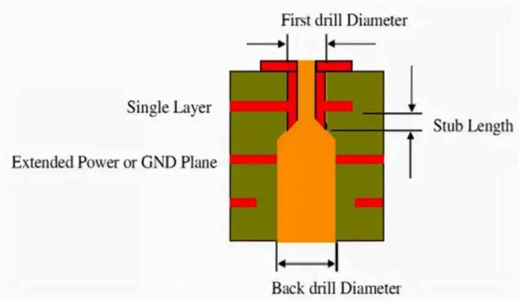
3D packaging semiconductor technology, also known as three-dimensional integrated circuit packaging technology, is an advanced semiconductor packaging method that allows multiple chips to be stacked together in a vertical direction to provide higher performance, smaller package size and lower energy consumption.
The core of this packaging technology lies in the stacking of multiple chips in the vertical direction, rather than the traditional planar arrangement of chips in a 2D package. This stacking helps to reduce the package area, improve the connectivity between electronic components, and shorten the signal transmission distance.
Due to the vertical stacking of chips, 3D packaging technology can reduce signaling delays and increase the bandwidth of data transmission, thus significantly improving the overall performance of the system.
3D packaging uses two primary methods to place multiple chips on top of each other: silicon through vias (TSVs) with microbumps and bump-free hybrid bonding. The former involves vertical electrical connections through silicon chips or wafers, while the latter utilizes dielectric bonding and embedded metals. This stacking enhances memory and processing power, making it suitable for data center servers, graphics gas pedals and networking equipment.
Fan-out packages redistribute connections and solder balls beyond the edge of the chip, resulting in a smaller form factor and improved thermal management. Fan-out packages are widely used in mobile applications due to their compact size and thermal resistance, making them a key player in the semiconductor market.
3D packages allow for the integration of more chips and functions per unit volume, enabling high capacity and high density packages. Shorter signal transmission distance and optimized power supply and heat dissipation design enable 3D packaging technology to reduce system power consumption. 3D packaging technology can integrate chips with different processes and functions to achieve multi-functional and high-efficiency packaging.
Wafer-level 3D packaging is a technology for packaging at the wafer level, and its main structure includes molded chip components with redistribution layers, called wafer-level CSP (WLCSP). In addition, 3D package structures typically have stacked cores with through-silicon vias (TSVs) and microbump interconnections, as well as face-to-face interconnections with microbumps for two cores. These structures enable wafer-level 3D packages to achieve higher performance, smaller size, lower power consumption, and better reliability.
The main features of wafer-level 3D packaging include:
- high efficiency: wafer-level 3D packaging can be packaged at the wafer level, thus improving packaging efficiency and reducing costs.
- smaller, thinner, lighter: wafer-level 3D packaging can achieve smaller, thinner, lighter electronic products to meet consumer demand for thin and portable.
- Higher performance: Wafer-level 3D packaging can achieve higher performance, improve the operating speed and processing power of electronic products.
- Lower power consumption: Wafer-level 3D packaging can achieve lower power consumption and extend the battery life of electronic products.
- Better Reliability: Wafer-level 3D packaging can improve the reliability of electronic products, reduce the failure rate, and improve product life.
IC Chips are made from hundreds of wafer processes to realize various functions,but their base material is silicon.Silicon itself is as fragile as a piece of glass, and the structures formed after multiple wafer processes are just as susceptible to mechanical and chemical damage.Therefore,packaging materials are critical to protecting the chip.
In addition, the semiconductor package is responsible for electrically and mechanically connecting the chip to the system. The package electrically connects the chip to the system, provides power to the chip, and also creates a pathway for signal input and output. At the same time, chips require a reliable mechanical connection from the outside world to ensure that they remain physically connected to the system during use.
At the same time, packages need to quickly dissipate the heat generated by semiconductor chips and devices.When a semiconductor product is in operation, current flows. This inevitably creates resistance,which then generates heat.If a semiconductor package does not dissipate heat effectively,the chip may overheat, causing the internal transistors to overheat and fail to operate.Therefore,it is essential for semiconductor packages to dissipate heat effectively. As semiconductor products evolve at a faster rate and with more functions,the cooling function of the package becomes more and more important.
Advantages
Allows integration of various components and functions in the most compact manner, making it possible to create highly complex systems in a compact form factor.
Improved vertical alignment of heat sink chips enables efficient heat dissipation to address the thermal challenges associated with high performance computing.
Interconnect lengths are further reduced (beyond 2.5D) to minimize signal delay and power consumption. A very significant advantage of 3D packaging technology is the reduction in distance. In a stacked structure, the distance between individual components is approximately 0.7 of the distance in a 2D structure. this reduction in distance directly impacts the power consumption in the wiring portion of the system as it results in less capacitance. As a result, the power consumption is now approximately 0.7 times higher than in the 2D configuration.
Applications
Increasingly popular in applications where extreme performance and miniaturization are critical. It is often used in advanced memory technologies such as High Bandwidth Memory (HBM) and advanced processors for high-end smartphones, gaming consoles and professional computing.
3D packaging semiconductor technology is reshaping the electronics industry with unprecedented potential for efficient integration, superior performance and miniaturization, heralding endless possibilities for the future of electronics. As the technology continues to evolve, it will be a key driver of industry growth!