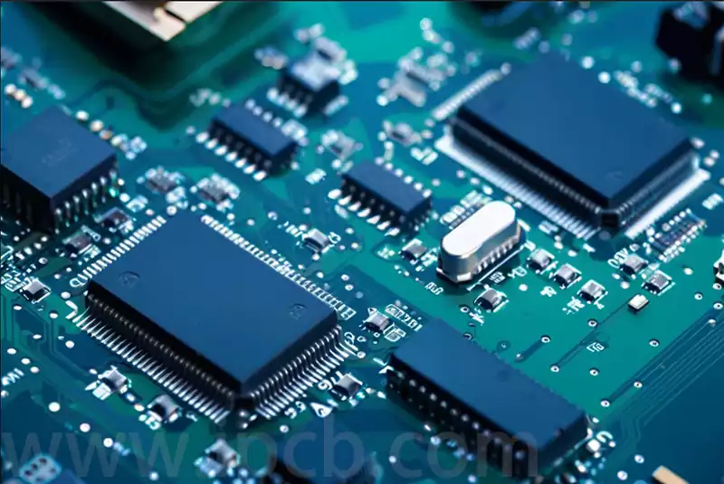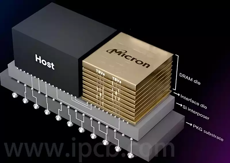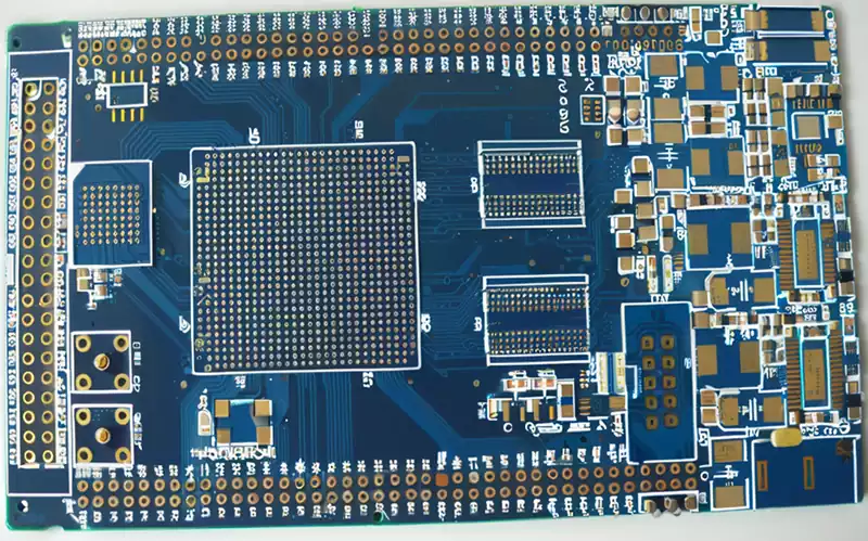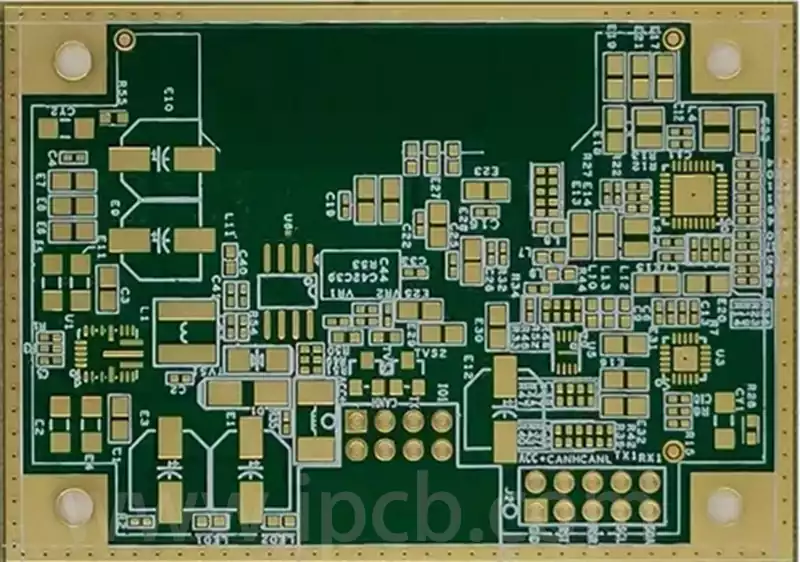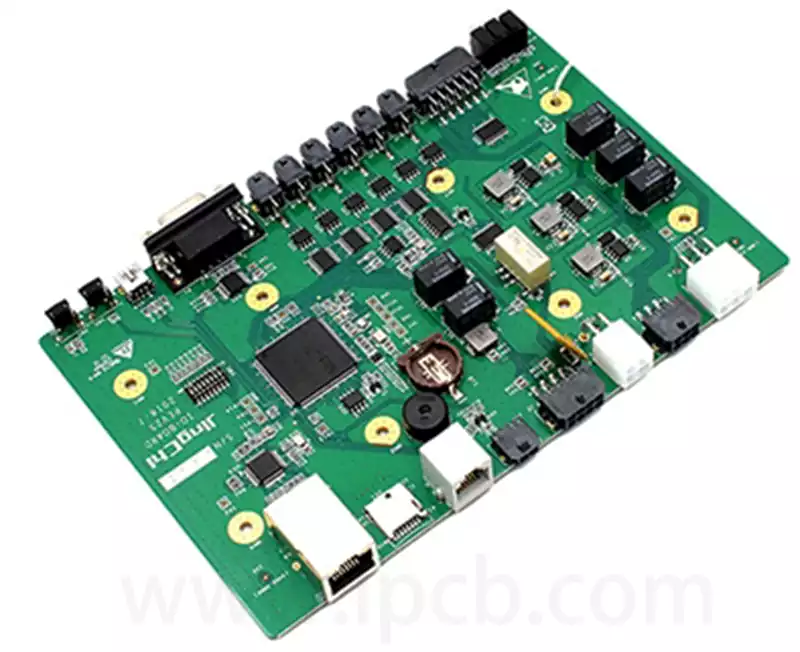
Key considerations and applications for high speed digital pcb
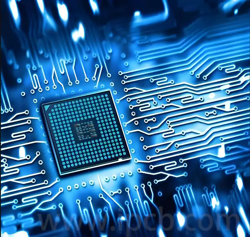
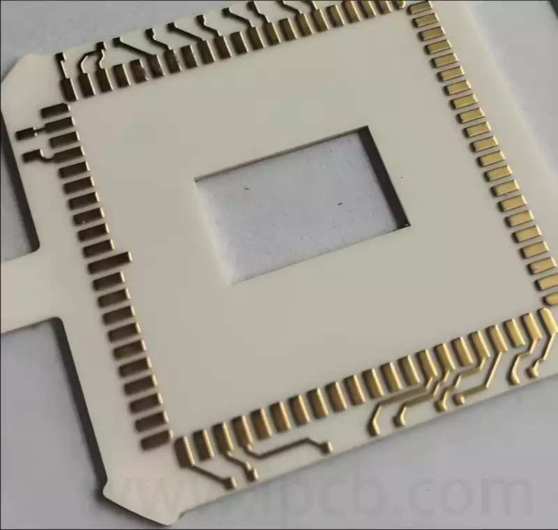
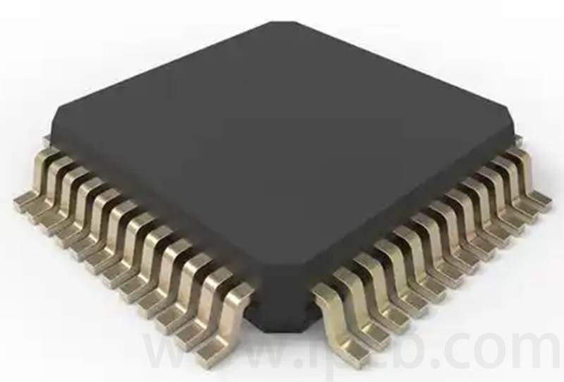
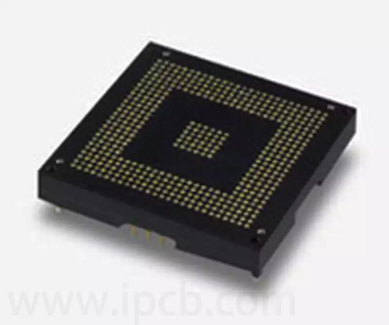
High speed digital pcb is circuit boards that can support high speed digital signal transmission, and are usually used in scenarios where the frequency of digital logic circuits reaches or exceeds 45MHz-50MHz, or where the delay of digital signals in circuits on the transmission line is greater than 1/2 rise time. Compared to traditional analogue […]