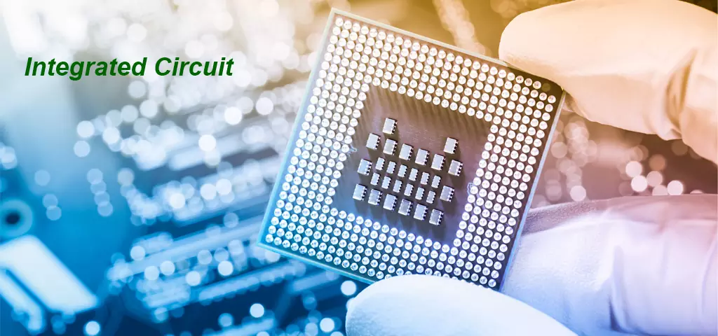
Integrated circuit = IC, an IC is a type of microelectronic device that developed in the late 1950s to 1960s as a new type of semiconductor device. It is an electronic device that undergoes semiconductor manufacturing processes such as oxidation, photolithography, diffusion, epitaxy, and aluminum evaporation, integrating all the semiconductor, resistor, capacitor, and other components required to form a circuit with certain functions, as well as the connecting wires between them, onto a small piece of silicon wafer, and then soldered and packaged in a shell. Its packaging shell comes in various forms such as round shell, flat, or double inline. Integrated circuit technology includes chip manufacturing technology and design technology, mainly reflected in the ability of processing equipment, processing technology, packaging testing, batch production, and design innovation.
All components in an integrated circuit boards have formed a cohesive structure, taking a big step towards miniaturization, low power consumption, intelligence, and high reliability in electronic components. It is represented by the letter IC in the circuit. Nowadays, integrated circuits have played a very important role in various industries and are the cornerstone of modern information society. Silicon integrated circuits are mainstream, which refers to the integration of various components required to achieve a certain function in a circuit onto a single silicon wafer, forming a whole called an integrated circuit.
Why does an ic pcb come into being? The world’s first electronic computer was born in the United States in 1946. It was a behemoth that covered an area of 150 square meters and weighed 30 tons. The circuits inside used 17468 electronic tubes, 7200 resistors, 10000 capacitors, 500000 wires, and consumed 150 kilowatts of electricity. Obviously, its most intuitive and prominent problem is its large footprint and inability to move. Damer, a scientist at the British Radar Research Institute, proposed at a meeting in 1952 that discrete components in electronic circuits could be assembled on a single semiconductor chip, and a small piece of chip would form a complete circuit. This would greatly reduce the size of electronic circuits and improve their reliability. This was the initial concept of integrated circuits, and the invention of transistors made this idea possible. In 1947, the first transistor was manufactured at Bell Laboratories in the United States. Prior to this, achieving current amplification could only rely on large, power-consuming, and structurally fragile electronic tubes. Transistors have the main functions of electronic tubes and overcome the aforementioned drawbacks of electronic tubes. Therefore, after the invention of transistors, the concept of semiconductor-based integrated circuits quickly emerged, and integrated circuits were quickly invented. Jack Kilby and Robert Noyce respectively invented germanium integrated circuits and silicon integrated circuits between 1958 and 1959.
There are many classification methods for integrated circuits, which can be divided into analog integrated circuits, digital integrated circuits, and mixed signal integrated circuits (analog and digital on the same chip) according to whether the circuit belongs to analog or digital.
Digital integrated circuits can contain anything from thousands to millions of logic gates, triggers, multitasking machines, and other circuits on a few square millimeters. The small size of these circuits allows for higher speed, lower power consumption, and reduced manufacturing costs compared to board level integration. These digital ICs, represented by microprocessors, digital signal processors (DSPs), and microcontrollers, use binary to process 1 and 0 signals during operation.
Analog ic circuit board include sensors, power control circuits, and operational amplifiers, which process analog signals. Complete functions such as amplification, filtering, demodulation, and mixing. By using simulation integrated circuits designed by experts with good characteristics, the burden of circuit designers is reduced, and there is no need to design from the basic transistors.
IC can integrate analog and digital circuits on a single chip to make devices such as analog-to-digital converters (A/D converters) and digital to analog converters (D/A converters). This type of circuit provides smaller dimensions and lower costs, but caution must be taken when dealing with signal conflicts.
Integrated circuits can be divided into TV integrated circuits, audio integrated circuits, DVD player integrated circuits, video recorder integrated circuits, computer (microcomputer) integrated circuits, electronic keyboard integrated circuits, communication integrated circuits, camera integrated circuits, remote control integrated circuits, language integrated circuits, alarm integrated circuits, and various specialized integrated circuits according to their purposes.
IC packaging refers to the process of connecting circuit pins on a silicon wafer to external connectors using wires for connection with other devices. The packaging form refers to the outer shell used for installing semiconductor integrated circuit chips. It not only plays a role in installation, fixation, sealing, protecting the chip, and enhancing the electric heating performance, but also connects to the pins of the packaging shell through the contacts on the chip, which are then connected to other devices through the wires on the printed circuit board, thereby achieving the connection between the internal chip and the external circuit. Because the chip must be isolated from the outside to prevent impurities in the air from corroding the chip circuit and causing a decrease in electrical performance.
IC packaging substrate not only provide support, heat dissipation, and protection for chips, but also provide electronic connections between chips and PCBs, playing a bridging role. They can even embed passive and active devices to achieve certain system functions.
With the rapid development of the electronics industry, the types of IC packaging processes are becoming increasingly diverse, and the steps and methods of different IC packaging processes are not the same. The development process of IC packaging technology has roughly only gone through the following stages:
Structural aspect: TO-DIP-PLCC-QFP-BGA-CSP;
In terms of materials: metal, ceramic ceramic, plastic plastic;
In terms of pin shape: long lead straight insertion – short lead or no lead mounting – spherical protrusions;
Assembly method: through-hole insertion surface assembly direct installation.
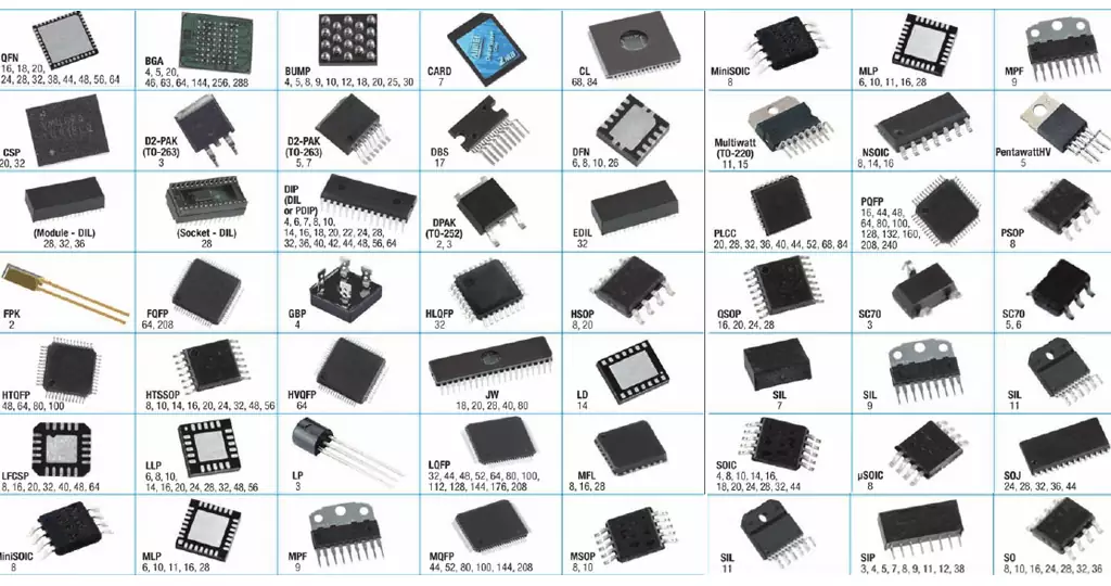
Several commonly used IC packaging processes
The Transistor Outline Package (TO package) process is the earliest type of transistor packaging process. TO packaging can be simply understood as a single side pin inline packaging. The TO packaging process can set different pin numbers according to the requirements of the IC, usually between 2-12, with 10 pin TO packaging being the most common.
Flat Package is another name for QFP or SOP. Four side pin flat package. One of the surface mount packages, with pins leading out from four sides in a seagull wing (L) shape. There are three types of substrates: ceramics, metals, and plastics. In terms of quantity, plastic packaging accounts for the vast majority. Plastic FP is the most popular multi pin LSI packaging. Not only used in digital logic LSI circuits such as microprocessors and gate arrays, but also in analog LSI circuits such as VTR signal processing and audio signal processing. In QFP, pins with a center to center distance of less than 0.65 mm are called FP.
Double Inline Package (DIP). One of the plug-in packaging types, with pins leading out from both sides of the packaging, and packaging materials available in plastic and ceramic. DIP packaging is currently one of the most popular plug-in packaging, with applications including standard logic ICs, memory LSIs, and microcomputer circuits. The center to center distance of the pins is 2.54 mm, and the number of pins is 6-64. The package width is usually 15.2 mm.
Plastic Led Chip Carrier (PLCC) is a plastic chip carrier with leads and a plastic J-lead chip packaging. One of the surface mount packaging types. The pins are led out from the four sides of the package in a T-shape and are plastic packaging. The shape is square, with a center to center distance of 1.27 mm between pins. The number of pins is 18-84, with 32 pins being more commonly used. The PLCC package has pins all around, and the overall size is much smaller than that of the DIP package. PLCC packaging is suitable for installing and wiring on printed circuit board using SMT technology (surface mount technology), and has the advantages of small size and high reliability. Widely used in circuits such as logic LSIs, DLDs (or Chen logic devices).
Plastic Quad Flat Package (PQFP). The spacing between chip pins in PQFP packaging is very small, and the pins are very thin. This packaging is generally used in large-scale or ultra large scale integrated circuits. The number of pins in PQFP is generally above 100.
Thin Small Outline Package (TSOP) is a thin, small-sized package. The typical feature of TSOP memory packaging technology is to make pins around the packaged chip. TSOP is suitable for installing and wiring on PCB boards using SMT technology. The TSOP package has a small external size and small parasitic parameters (voltage disturbances caused by significant changes in current), making it suitable for high-frequency applications. Easy to operate and highly reliable.
Ball Grid Array Package (BGA). One of the surface mount packaging types. Create spherical protrusions on the back of the printed substrate in an array pattern to replace pins, assemble an LSI chip on the front of the printed substrate, and then seal it with molded resin or potting method. Also known as Convex Array Carrier (PAC). Pins exceeding 200 are a packaging process used for multi pin LSIs. The use of BGA packaging technology in memory can increase memory capacity by 2 to 3 times while maintaining the same volume. Compared with TSOP packaging, BGA packaging can achieve smaller results, and at the same capacity, the former has only one-third the volume of the latter. In addition, compared with traditional TSOP packaging process, BGA packaging process has a faster and more effective heat dissipation pathway. And, BGA packaging does not have to worry about pin deformation issues like TSOP packaging. The I/O terminals in BGA packaging are distributed in an array of circular or columnar solder joints below the packaging. The advantage of BGA technology is that although the number of I/O pins increases, the pin spacing does not decrease but instead increases, thereby improving the assembly yield. In addition, although its power consumption increases, BGA can be soldered using a controllable collapse chip method, which can improve its thermoelectric performance. The thickness and weight of BGA packaging have been reduced compared to previous packaging technologies, with reduced parasitic parameters, low signal transmission delay, and significantly increased usage frequency. The assembly of BGA packaging can be achieved through coplanar welding, which improves reliability.
More and more circuits are appearing in the hands of designers in the form of integrated chips, leading to a trend towards miniaturization and high-speed development in electronic circuits. More and more applications have been transformed from complex analog circuits to simple digital logic integrated circuits. Integrated circuit have become ubiquitous, and computers, mobile phones, and other digital appliances have become an indispensable part of the modern social structure. This is because modern computing, communication, manufacturing and transportation systems, including the Internet, all depend on the existence of integrated circuit. The digital revolution brought about by integrated circuit is the most important event in human history.
