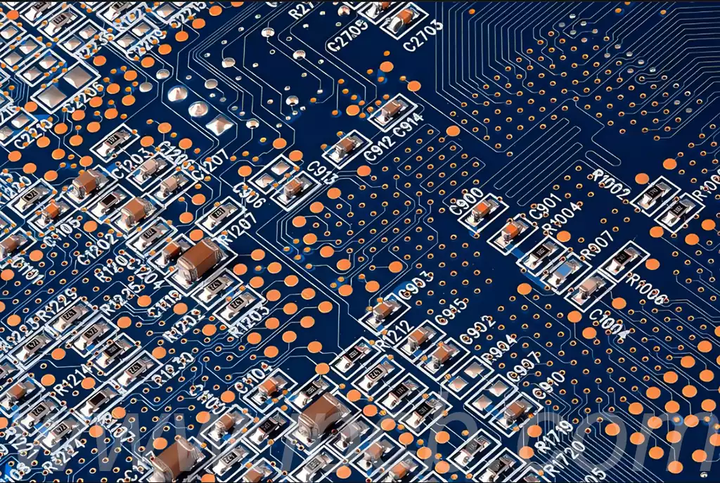
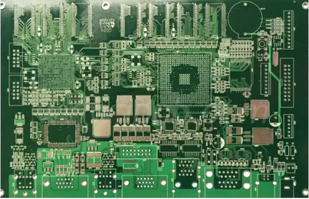
What is hasl pcb finish?HASL PCB, known as Hot Air Solder Leveling (Hot Air Solder Leveling) for Printed Circuit Board (Printed Circuit Board), is a surface treatment technology used in the PCB manufacturing process.
Tin spraying process known as HASL hot air leveling, also known as hot air solder leveling, it is coated with molten tin-lead solder on the surface of the PCB board and heated compressed air leveling (blowing) process, so that the formation of a layer of copper oxidation resistance can also provide good solderability coating layer, hot air leveling leveling of solder and copper in the combination of the formation of copper-tin metal compounds, the thickness of about 1 ~ 2 mil.
PCB hot air leveling level to be immersed in molten solder, the wind blade in the solder solidified before blowing the liquid solder, and can be solder on the copper surface of the solder to minimize the bending of the moon shape and prevent solder bridging.
Hot air leveling is divided into vertical and horizontal two kinds, generally believe that the horizontal type is better, mainly because of the horizontal hot air leveling plating layer is more uniform, can realize automatic production. The general process is as follows: micro-etching –> preheating –> flux coating –> tin spraying –> cleaning.
HASL finish pcb needs to master the following important parameters: welding temperature, air knife wind temperature, air knife pressure, dip welding time, lifting speed, etc..
Improvement of soldering quality
Hot air solder leveling can effectively remove the oxidized layer, oil, dust and other impurities on the surface of the pad, making the pad surface cleaner and flatter, thus improving the quality of soldering. At the same time, hot air solder leveling can also make the pad surface form a thin layer of solder film, which helps to improve the wettability of the solder and reduce the occurrence of false soldering, leakage and other problems.
Reduce production cost
Hot air solder leveling can effectively reduce the defects in the soldering process, thus reducing the rework rate and the generation of scrap. In addition, hot air solder leveling equipment has a long service life and low maintenance cost, which can save a lot of equipment investment cost for enterprises.
Advantages of Hot Air Solder Leveling (HASL):
Sufficient availability; rework is possible;
Outstanding shelf life;
Excellent solderability;
Cheap/low cost;
Allows for larger processing windows;
Longer storage time;
PCB is completed with pads completely covered with tin before soldering;
Suitable for lead-free soldering;
Proven surface finish options;
Allows for visual inspection and electrical measurements
Disadvantages:
Uneven surface;
Not suitable for fine pitch;
Contains lead (HASL);
Thermal shock;
Solder bridging;
Plugged or reduced PTH (Plated Through Hole);
Thickness/form differences between large and small pads;
Not suitable for SMDs and BGAs with less than 20 million pitch;
Not suitable for HDI products;
Not suitable for wire bonding.
Tin spraying process is divided into leaded tin spraying and lead-free tin spraying, the difference is that lead-free tin spraying belongs to the environmental protection class process, does not contain hazardous substances “lead”, melting point of about 218 degrees; leaded tin spraying does not belong to the environmental protection class process, contains hazardous substances “lead”, melting point of about 183 degrees. From the surface of tin, leaded tin is brighter and lead-free tin is duller.
Leaded tin
The so-called leaded tin spray refers to the tin according to a certain ratio, modulation and become, lead will improve the activity of the tin wire in the soldering process, leaded tin wire is relatively better than the lead-free tin wire, but the lead is toxic, lead lead in the lead is harmful to the human body; leaded eutectic temperature is lower than the lead-free. Specifically how much depends on the composition of the lead-free alloy ah, like SNAGCU eutectic is 217 degrees, the soldering temperature is the eutectic temperature plus 30 ~ 50 degrees. Depends on the actual adjustment. Leaded eutectic is 183 degrees. Mechanical strength, brightness, etc. Leaded is better than lead-free. So leaded tin is not environmentally friendly, and the world promotes environmental protection has a certain discrepancy. Therefore, lead-free spray tin was born.
Lead-free tin spraying
Lead-free tin is an environmentally friendly process, it is very harmless to the human body is also a process advocated at this stage, lead-free tin for the lead content of no more than 0.5, lead-free tin will be a high melting point, so that the soldering point is much stronger. In essence, leaded tin and lead-free tin is a process. It is only the purity of lead that is different. Lead-free tin for the human body for the environment is more environmentally friendly and safer, but also a future development trend, it is recommended that we use.
PCB tin spraying process flow
1.Preparation
PCB spraying tin, first need to thoroughly clean the PCB board edge of dust, oil, etc., and then the appearance of the inspection to ensure that the PCB no scratches, no impurities, no defects into the next process.
2.Pre-tin spray treatment
Coating soldermask: Coating soldermask in the areas that need to retain the insulation properties, to prevent these areas from being covered when spraying tin.
Exposure and development: The conductive areas to be tinned are exposed through the exposure and development process.
3.Tin spray construction
First, select the appropriate tin spray equipment and tin spray material, and ensure that the equipment is in good condition.
Then, set the tin spray parameters, according to the PCB material, thickness, conductive and customer demand and other factors, set the tin spray pressure, speed, temperature and other parameters.
Finally, start tin spraying, put the PCB into the tin spraying equipment, start the tin spraying program. During the process of tin spraying, according to the effect of tin spraying, real-time adjustment of tin spraying parameters to ensure the quality of tin spraying.
4.Post-tinning
Check the quality of tin spraying: Check the circuit board after tin spraying to ensure that the effect of tin spraying meets the requirements.
Cleaning and drying: Remove the residue generated during the process of tin spraying, and then dry the PCB.
5.Precautions
During the operation process, the construction personnel should pay attention to protection, wear protective glasses and gloves to avoid skin and eye damage. At the same time to keep the construction environment clean, dust-free, and construction equipment positioning maintenance and maintenance and testing and calibration.
With its unique hot air solder leveling technology, HASL PCB plays an important role in improving soldering quality, reducing costs and meeting environmental protection needs. With the continuous advancement of technology, this pcb finish surface technology will continue to occupy an important position in the electronics manufacturing industry and contribute to the development of the industry.