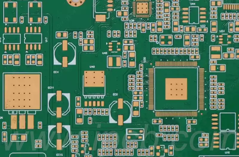
The use of open source hardware and its supporting open source schematics and PCB layouts has become a notable trend in the field of electronic design. This trend not only improves engineers’ productivity and reduces time-to-market, but also fosters innovation and collaboration in the electronic design field. This trend is expected to grow further as engineers deepen their understanding of the differences between traditional PCBs and source pcb.
Source PCB design offers multiple advantages over traditional PCB design. Among them, the repeated availability of power and digital components as well as high-speed data components is particularly impressive. This makes engineers more inclined to adopt open source PCB design. In the past, engineers often faced power layout challenges during the design process. In open source designs, the boards are faster and equipped with RF architectures, making the power layout more complex and requiring more attention from engineers. In an open source PCB design environment, as long as the layout is proven to work, it can be copied and used without having to redesign it from scratch.
As design needs grow, many engineers are accustomed to referring to application notes or seeking help from manufacturers, or even using PDF versions of circuit boards to measure wiring ratios on drawings. As a result, when faced with an application design that involves multiple complex layouts, engineers prefer open-source PCBs. the ease of use of open-source designs allows engineers to complete all modules of the PCB design process without having to become a layout expert. When encountering special problems, engineers will not feel the layout pressure. For example, for difficult power modules in traditional PCB design, the use of existing open source design solutions can simplify its layout. Complex PCB design layouts, such as power supplies, high-speed interfaces and circuits, and even impedance matching pcb layout, can be simply and quickly reused or replicated with open source designs.
However, open source designs also face some challenges, such as noise problems during integration. When boards use high-current switches, the noise can interfere in other circuits. In addition, perhaps the biggest challenge facing open source designs is the learning curve. While engineers can easily copy and paste open-source layouts, they may also lose the opportunity to learn the fundamentals of the complete design, including setting spacing, necessary line widths and impedance matching.
This puts the engineer in a dilemma: Not using an open source design may lead to certain component design issues during the design process, while using an open source design may not allow for in-depth design knowledge. If engineers cannot understand the basic principles of design, they will have a hard time meeting the unique design challenges ahead.
On the other hand, using open source designs can provide engineers with valuable experience about the PCB design process. In other words, the learning barriers created by using open source design can be transformed into real learning opportunities if done correctly.
Using open source designs can serve as a starting point for engineers to learn about design. If engineers use open source layouts as a reference point, then they can dive deeper into their PCB design knowledge. From this reference point, engineers can reflect to better understand why certain layouts utilize specific layout methods. This provides a new way for engineers to learn from existing designs that traditional PCB design models cannot provide.
In the case of power supply designs, for example, if engineers use open source layouts during the design process, they can backtrack from the results to the design process based on the specific components, wire spacing, and number of copper wires used in the power supply design. This provides an excellent opportunity for engineers to learn design fundamentals, including thermal management, impedance matching, and power supply layout, from a hands-on approach.
However, engineers must be careful when deciding whether to use open source designs. Not all open source designs are validated. For example, some engineers may create open source layouts without fully considering their applicability to other engineers’ design layouts. In the case of thermal management of an open source design, for example, the design may fail if the engineer does not fully understand the differences between the design options. In short, sometimes we don’t know the source of the open source layout being used, making it difficult to predict its reliability.
Once again when designing power modules based on open source layouts, engineers may encounter some problems. Initially, the engineer may think the board is working fine and integrate it into the design. However, when it comes to the testing phase, it may turn out that the initial design was not fully tested to meet specific specifications or requirements, such as electromagnetic interference (EMI) caused by radiation or conduction.
Fortunately, engineers using an open source layout for the first time can refer to the following recommendations. The transistor supplier’s layout in the source PCB layout may be more robust and reliable than the layout in the online bulletin. Just as engineers in open-source discussion groups like to gather on platforms for discussions, engineers in the PCB design industry see forums as one of the gateways to discuss the successes and failures of specific open-source layouts. As electronic design methodologies shift to the open source model, it is important that we clearly recognize the challenges, the advantages and the unique learning opportunities that open source offers. This will not only benefit engineers and manufacturers, but will also provide a strong boost to the PCB industry as a whole.