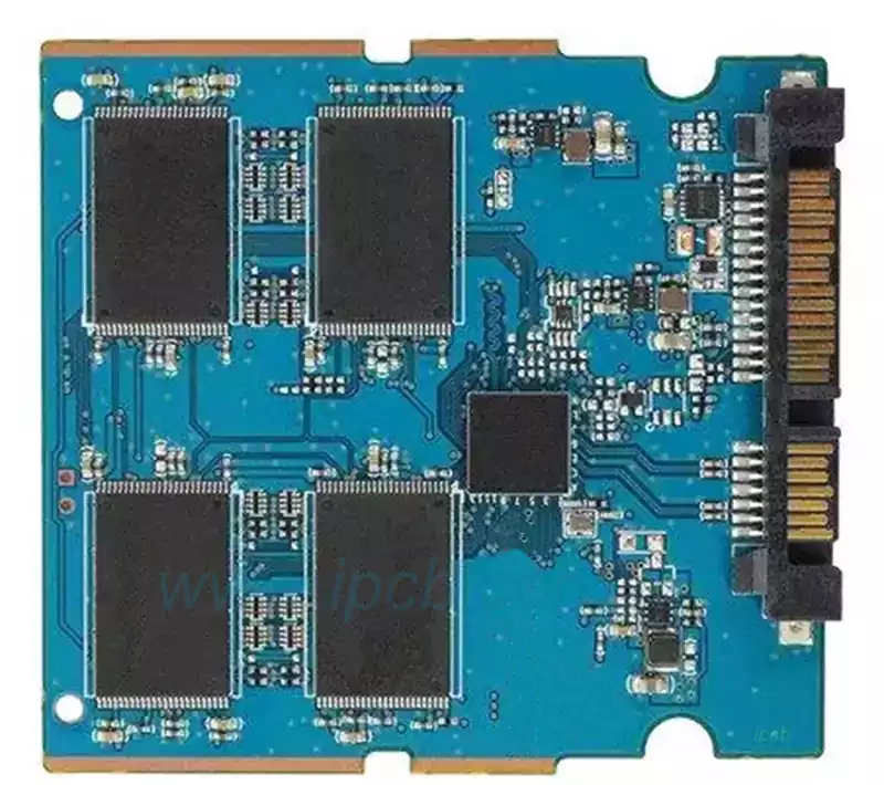
The hard disk pcb board is the core component in a hard disk drive and is responsible for connecting and controlling the various functions of the hard disk. It is mainly composed of a microprocessor, cache memory, motor drive circuitry and interface circuitry, etc. These components work together to ensure that the hard disk is able to read and write data accurately.
The main functions of the hard disk pcb board include:
Data Read/Write Control: The board is responsible for controlling the data read/write process, ensuring that data is accurately read from the hard disk to the memory or written from the memory to the hard disk.
Motor Drive: Inside the hard drive are one or more disk platters that need to rotate at high speeds to ensure stable reading and writing of data. The motor drive circuitry on the hard drive circuit board is responsible for controlling the rotation speed of these disk platters.
Error Detection and Correction: The boards have powerful error detection and correction capabilities that can automatically detect errors in the data and correct them in a timely manner to ensure data integrity and accuracy.
The general process flow of hard disk circuit board manufacturing:
Material Preparation: First of all, you need to prepare the raw materials needed to manufacture the circuit board, including insulating materials, conductive materials, copper foil and so on. These materials need to undergo strict quality checks to ensure that they meet the manufacturing requirements.
Copper Foil Pasting: Paste the copper foil onto the insulating material to form the substrate of the pcb board. Professional equipment and processes are required to ensure that the copper foil is tightly bonded to the insulating material without air bubbles or warping.
Circuit pattern design: According to the requirements of circuit design, use professional design software to draw circuit patterns. The circuit pattern needs to take into account the connection relationship of the circuit, component layout, wiring optimization and other factors to ensure the performance and stability of the circuit board.
Photolithography: The designed circuit pattern is transferred to the circuit board, and the circuit pattern is exposed to the circuit board through a photolithography machine. The photolithography process requires the use of professional photoresist and exposure equipment to ensure the accuracy and clarity of the circuit pattern.
Etching: After photolithography, the circuit board will form a layer of photoresist protective film, which needs to be etched through the etching process will not be protected by the photoresist copper foil etching off, the formation of circuit patterns. Etching process requires the use of etching solution and professional etching equipment to ensure the uniformity and consistency of etching.
Drilling: Drill holes in the circuit board to insert components into the circuit board. The drilling process requires the use of specialized drilling equipment and drills to ensure that the location and size of the holes are accurate.
Soldering: Solder the components to the circuit board to complete the circuit connection. The welding process requires the use of professional welding equipment and welding materials to ensure the quality and reliability of welding.
Testing and inspection: After completing the welding, the circuit board needs to be tested and inspected to ensure that its performance and stability meet the requirements. The testing process requires the use of professional testing equipment and testing methods, comprehensive and accurate testing of the circuit board.
Hard disk pcb board is an important part of the hard disk drive, its performance and stability for the overall performance of the hard disk and data security is critical.