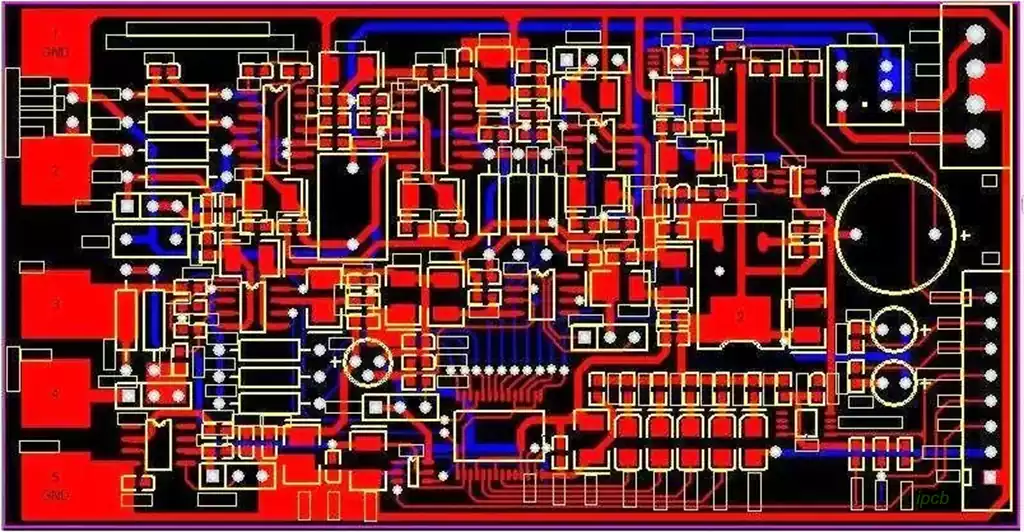
In the manufacturing process of electronic equipment, pcb layout is a crucial link. A reasonable circuit board layout can ensure the efficient and stable operation of electronic equipment, but also help to improve production efficiency and reduce production costs!
Seven principles of device layout in circuit board design
Convenience
In the circuit board design will often be applied to potentiometers, adjustable capacitors, key switches, adjustable inductors and other adjustable devices, such devices we may want to adjust them after the design of the whole board, some devices such as keys may also become the board’s open button so that such devices in the design of the board to be placed on the edge of the board or in other easy-to-access places.
Stress principle
In the design, such as a variety of USB interfaces, emulation of the downloader interface or other plug-in devices, because it requires a large force to plug, in order to prevent stress concentration on the circuit board caused by the risk of irreparable, usually these devices are arranged in the center of the board on the axis of symmetry.
Principles of heat dissipation for high-power devices
In the layout of the circuit board if you encounter easy to heat components should be placed on the edge of the circuit board or other components of the region less, and sometimes also for the addition of heat sinks and other measures. At the same time, the temperature-sensitive devices away from the heating element, so as not to affect the accuracy and stability of the system.
Isolation principle
- If both analog and digital circuits exist in the circuit, the two circuits should be isolated by isolation devices and regionalized layout in modules.
- In the circuit at the same time there are low-frequency circuits and high-frequency circuits, on the basis of high-frequency circuits do not affect the high-frequency circuits, high and low-frequency circuits for isolation. 3. Circuits appear in the strong and weak telecommunication signals need to isolate the two signals, such as opto-coupler isolation, transformer isolation, etc., in order to prevent the strong power on the interference of the weak power.
Proximity principle
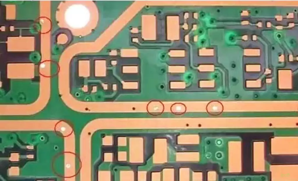
In the pcb board often exists 10uf capacitor and connected to 104 capacitors such as preventing voltage track collapse circuit, the two devices should be close to the possible next to the power port of the corresponding components. 2. As far as possible, the two high-frequency devices to keep the shortest possible connection line. 3. EMI filters should be kept as close as possible to the EMI source.
Aesthetics and manufacturability principles
Aesthetics refers to the design of the entire board should be kept sparse and dense, the core controller in the center of the rest of the sub-circuits are evenly distributed around it. Manufacturability refers to the design of the circuit board should take into account the processing capabilities of the foundry, and you should be in the soldering assembly components in the appropriate location and can be matched with the shell.
Ease of Replacement
The principle of easy replacement usually refers to the later maintenance of easy maintenance, crystal oscillators and other easily damaged devices in the layout should be considered easy to dismantle.
PCB layout considerations
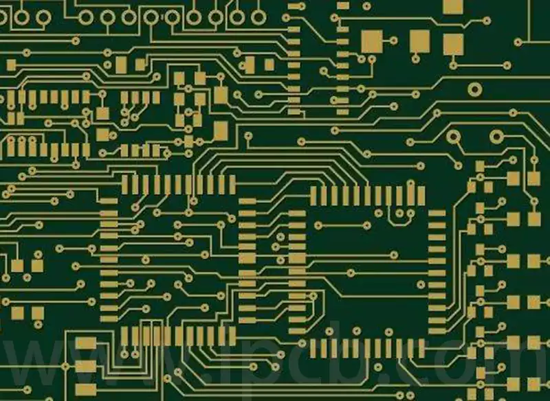
Avoid cross wiring: minimize or avoid cross wiring between components to reduce signal interference and improve the aesthetics of the wiring.
Wiring width and length: According to the size of the current and signal frequency, a reasonable choice of wiring width and length to ensure the stability and efficiency of signal transmission.
Grounding design: Reasonable grounding design is essential to improve the stability and anti-interference ability of the circuit board.
Avoid sharp corners and right angles: When wiring, try to avoid sharp corners and right angles to reduce electromagnetic interference and improve the quality of wiring.
Marking and recording: In the layout process, record the location of components and wiring information in a timely manner to facilitate subsequent production and maintenance.
PCB layout is an important task in the electronic manufacturing process. It not only requires engineers to have solid professional knowledge and a wealth of experience, but also requires them to use artistic and scientific methods, comprehensive consideration of various factors to ensure that the circuit board design is optimal.