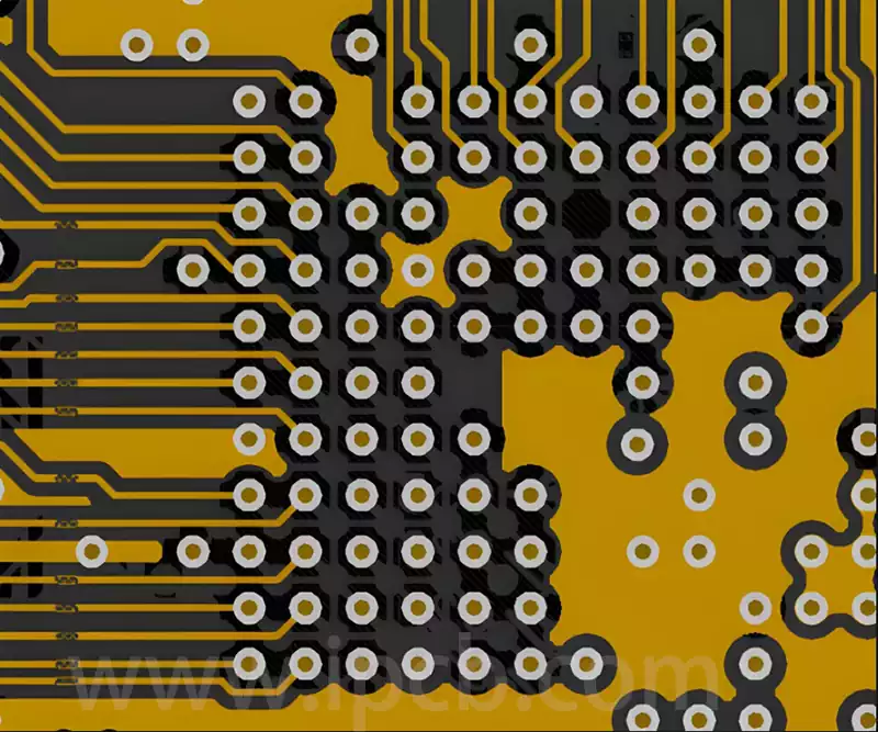
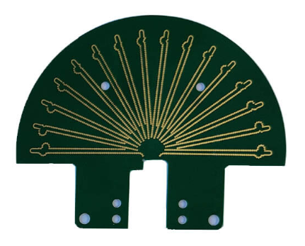
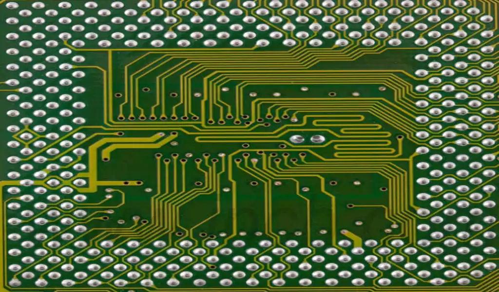
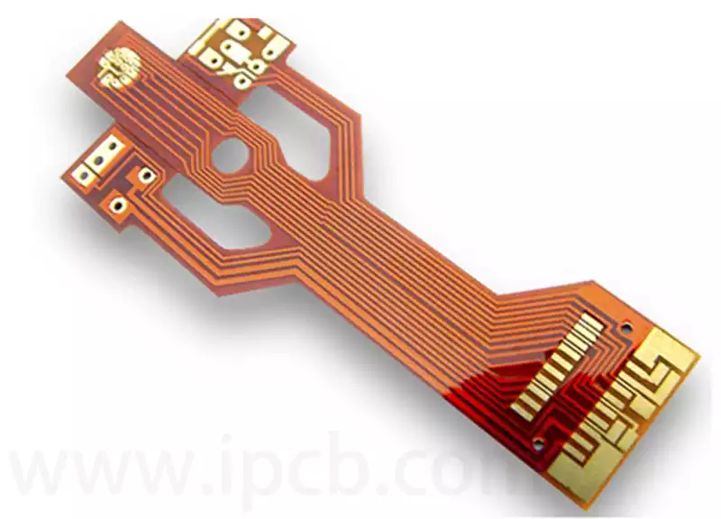
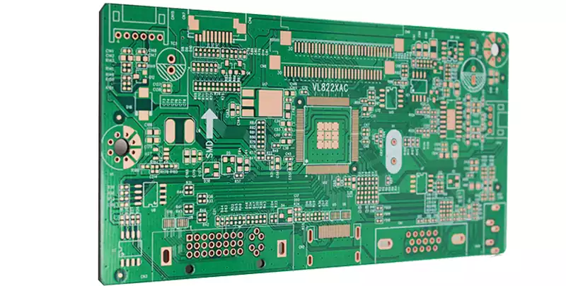
OSP meaning Organic Solderability Preservatives, the Chinese name is Organic Solderability Film or Copper Protector. The core concept is to chemically generate a layer of organic film on the clean bare copper surface. This film has multiple properties such as resistance to oxidation, thermal shock, and humidity, and its main function is to protect the copper surface of the circuit board from oxidation or sulfidation in the normal environment. However, in the subsequent soldering process, when encountered at high temperatures, this layer of protective film and must be able to be quickly and effectively removed by the flux, in order to expose the clean copper surface, so that it can be in a very short period of time and the molten solder tightly bonded to form a stable and reliable solder joints.
Main purpose
To enhance the reliability and stability of products by constructing a protective layer of antioxidant on PCB boards. In addition, the protective layer can effectively reduce the impact on subsequent processes such as drilling and assembly, ensuring the smooth running of the entire production process.
Process Flow
- Process flow: Degreasing → water washing → micro-etching → water washing → acid washing → pure water washing → OSP → pure water washing → drying.
- Principle: Form a layer of organic film on the copper surface of the circuit board, firmly protect the fresh copper surface, and at high temperatures can also prevent oxidation and pollution.OSP film thickness is generally controlled at 0.2-0.5 microns.
- Features: good flat surface, OSP film and circuit board pads of copper between the formation of no IMC, allowing welding solder and circuit board copper direct welding (good wettability), low-temperature processing, low cost (can be lower than the HASL), processing of energy use and so on. Can be used in low-tech circuit boards, but also available in high-density chip package substrate.
- OSP material types: rosin (Rosin), active resin (Active Resin) and azole (Azole).
- Shortcomings:
① Appearance checking is difficult, not suitable for multiple reflow soldering (generally require three times);
② film surface is easy to scratch
③ Higher storage environment requirement;
④ Shorter storage time; - Storage method and time: vacuum packaging for 6 months (temperature 15-35 ℃, humidity RH ≤ 60%);
- SMT site requirements:
① OSP circuit boards must be stored in low temperature and low humidity (temperature 15-35 ℃, humidity RH ≤ 60%) and avoid exposure to acid-filled environment, packaging unpacked within 48 hours after the start of assembly;
② single-sided on the piece is recommended to be used within 48 hours, and it is recommended to use a low-temperature cabinet to save without vacuum packaging to save;
③ DIP is recommended to be completed within 24 hours after the completion of both sides of the SMT;
Advantages
OSP significantly improves product reliability and stability. By forming an effective antioxidant protective layer on the surface of the PCB substrate, it successfully prevents the oxidation of copper surfaces, thus ensuring long-lasting and stable product performance.
In addition, OSP significantly reduces the potential impact on subsequent process steps. In drilling and assembly, the presence of the OSP layer reduces unnecessary complexity and potential risks, thus improving the overall process efficiency and quality.
Compared to traditional surface treatment processes, such as electroplating, OSP offers significant cost advantages. It not only reduces production costs, but also meets the sustainable development requirements of modern industry with its environmentally friendly characteristics, bringing real economic and environmental benefits to enterprises.
Scope of application
It is widely used in the manufacture and processing of PCB boards, including cell phones, computers, automobiles, home appliances and other fields. Meanwhile, it can also be applied to the manufacture and processing of other electronic products, such as smart wearable devices, IoT devices and so on.
OSP plating, as an important PCB board surface treatment process, has a wide range of applications and significant advantages. It will continue to play an important role in the future manufacturing of electronic products and promote the development of the industry.
