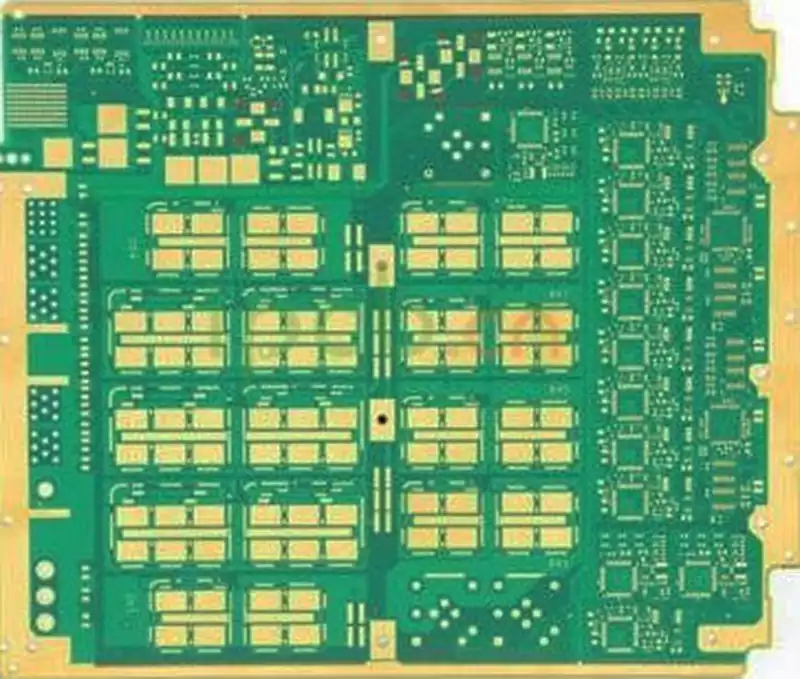
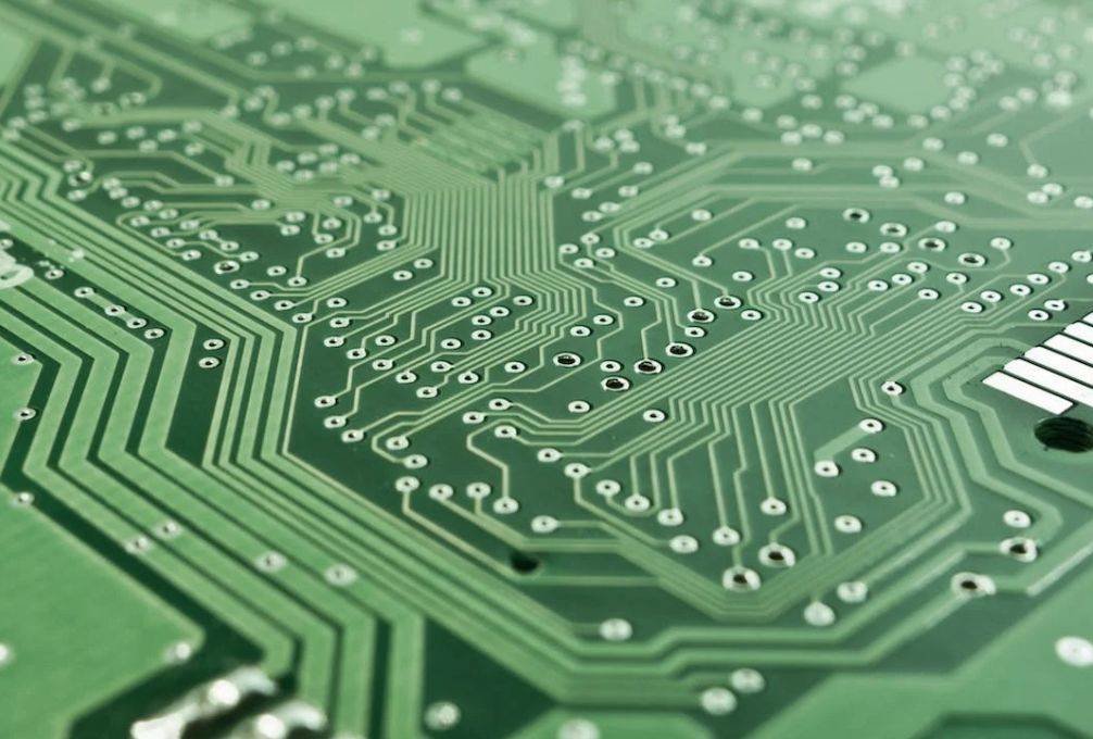
A glass PCB board is a printed circuit board that uses glass as its substrate. While traditional PCBs usually use paper or plastic substrates, glass substrate PCBs use glass as the substrate material.
Glass PCB board is widely used in electronic products that require high performance and reliability, such as flat panel displays, smartphones, and LED lighting. They can provide higher circuit density, better signal transmission performance and a more stable operating environment, as well as a longer service life and lower failure rate.
Mainstream processes for glass substrate manufacturing:
There are three main manufacturing processes for glass substrates: float, flow-hole down-lead and overflow melt, and the current mainstream process is the overflow melt method.
Float manufacturing process
Float manufacturing process is the most widely used and oldest flat glass manufacturing process. Molten glass from the pool kiln continuous inflow and floating in the relative density of the tin liquid surface, under the action of gravity and surface tension, the liquid glass in the tin liquid surface spread, spreading, the formation of the upper and lower surfaces of the flat, hardened, cooled by the transition rollers led to the table. The advantages of the float method are high production capacity and easy expansion of the substrate glass area size.
Flow Hole Pull Down
Flow hole pull down method is the molten glass solution into the platinum alloy process by the flow hole leakage plate groove, under the action of gravity glass solution outflow, and then through the roller mill, cooling room curing molding. The temperature and the size of the flow hole opening together determine the glass yield, while the size of the flow hole opening and the pull-down speed together determine the thickness of the glass, and the temperature distribution determines the flatness of the glass.
Overflow melting method
In overflow melting, molten glass is introduced into a conduit, and when the glass reaches the upper volume limit, it overflows from both sides of the conduit along the pipe wall, and like a waterfall, forms a sheet-like substrate at the lower end of the flow. Overflow melting technology can produce ultra-thin glass substrate with double original glass surface, compared with the float method and flow hole pull-down method, can be exempted from grinding or polishing and other post-processing production process, has become the mainstream of TFT-LCD substrate glass manufacturing process.
Advantages of glass substrate:
- Good thermal stability, can avoid the traditional copper-clad plate heat shrinkage, warping caused by the graphic positional accuracy problems, good for the latter part of the process of component mounting welding.
- Good heat dissipation performance, can effectively improve the problem of uneven local heat dissipation, reduce the loss of component life and display products, the loss of luminous efficiency.
- High flatness of the glass substrate, for some special products (such as the need to transfer a huge amount), can reduce the difficulty of chip transfer, improve the overall yield of finished products.
- Low cost of glass raw materials, bringing advantages in the comprehensive manufacturing cost of finished products; and glass raw materials are easy to obtain, recyclable, stable supply channels and prices.
Glass pcb board as the cornerstone of the modern electronics industry, its importance is self-evident. In the future, with the rapid development of flexible display, Internet of Things, artificial intelligence and other emerging technologies, it will usher in a broader development space and unlimited possibilities.