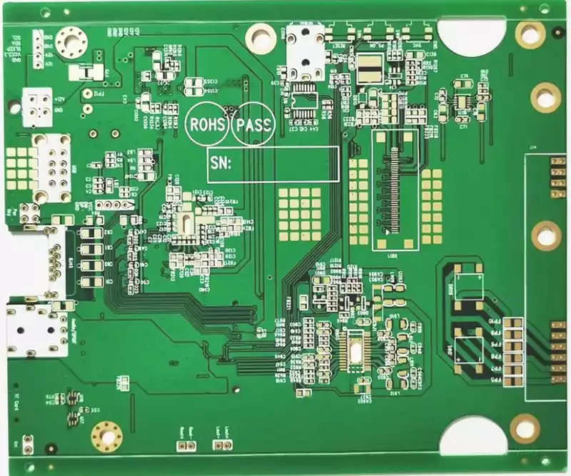
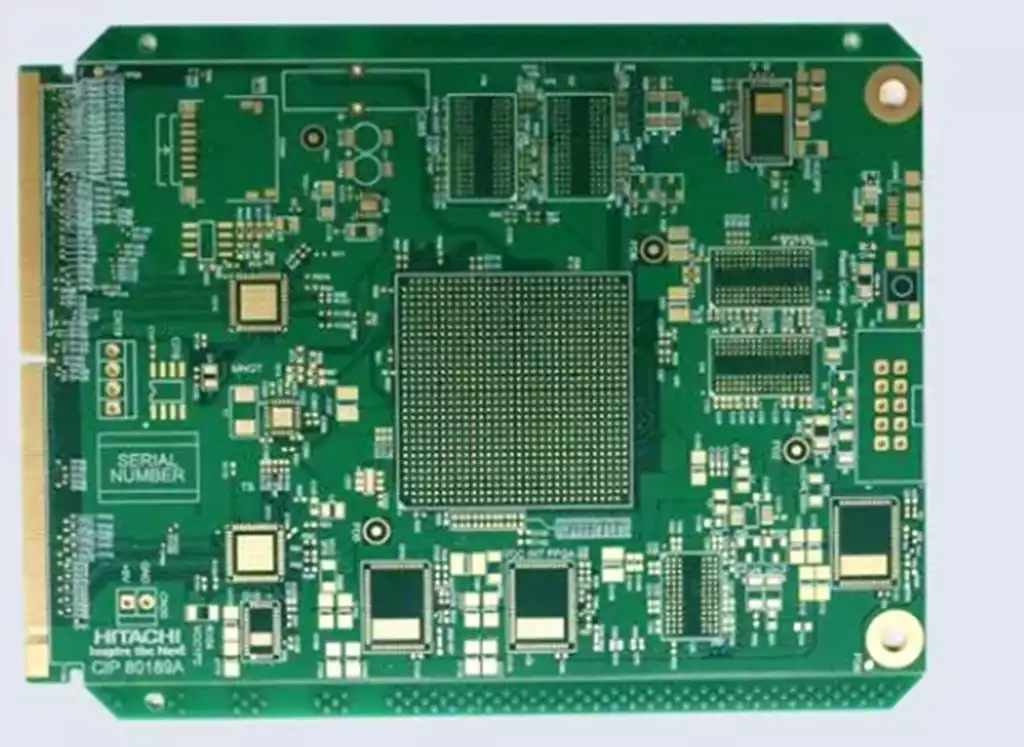
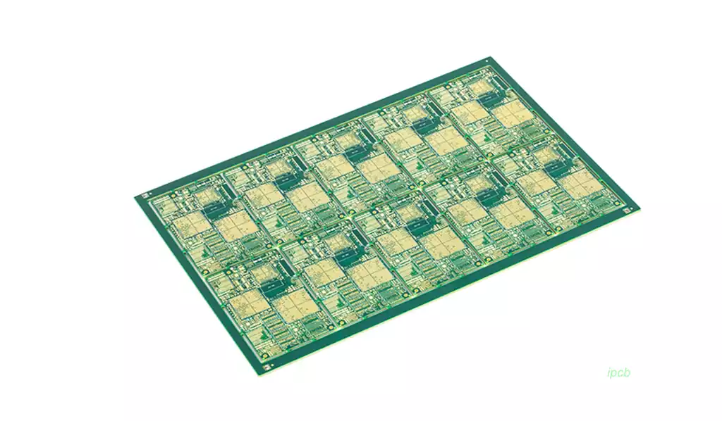
2step hdi board (High-Density Interconnect) is a high-density interconnect technology used primarily in electronic devices to achieve higher signaling speeds and smaller sizes.
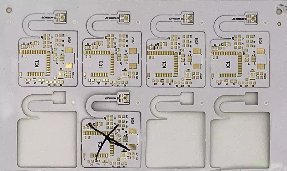
2step HDI board further increases the number of layers and the outer layer of copper from the basic first-order HDI structure, which gives second-order HDI a higher line density than first-order HDI. 2 step HDI boards typically contain four to six layers, including an outer copper layer, an inner copper layer, inner vias, and an isolation layer. The outer copper layer is used to provide more connection points and lines, while the inner copper layer is used for signaling and the inner vias are used to connect the inner and outer layers. This structure makes second-order HDI boards suitable for high-end electronic devices such as smartphones and tablets.
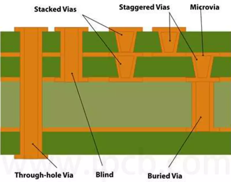
The manufacturing process for second-order HDI includes the use of laser drilling technology, in which the 2 step HDI boards are laser drilled twice. The manufacturing process is also very demanding due to its complexity and the use of several key technologies.
Copper plating is one of the key steps in the manufacturing process of HDI second order circuit boards. At this stage, the board needs to be immersed in a solution containing copper ions, which are deposited on the surface of the board through an electrochemical reaction to form a thin film of copper. This process requires precise control of the concentration, temperature and current density of the solution to ensure the uniformity and conductivity of the copper film. If there is a problem with the copper plating process, it may lead to a degradation of the circuit board’s electrical performance or even problems such as short circuits.
Next, etching is another important manufacturing step. In this process, an acidic or alkaline solution is used to dissolve away unwanted parts of the circuit board to form a predetermined circuit pattern. The precision with which the etching process is controlled directly affects the circuit density and aperture size of the board. Over or under etching can lead to degradation of the board’s performance.
Next, soldermasking is the process of shielding the parts of the circuit board that do not require soldering. In this process, a special layer of soldermask is applied to the surface of the board and then baked at a high temperature to cure it. The precision of the control of the soldermask process affects the quality of the soldering, and if the soldermask is uneven or incompletely cured, it may result in a less stable solder joint.
Finally, assembly is the process of soldering circuit boards together with other electronic components (e.g. chips, capacitors, etc.). This process requires precise control of soldering temperature and time to ensure the quality and stability of the solder joints. If there is a problem with the assembly process, it may lead to degradation of the board’s performance or even failure.
HDI boards offer many advantages, including the following:
- Higher line density: HDI boards can greatly increase the number of interconnected lines per unit area through blind buried holes and multilayer interconnect technology, thus increasing line density.
- Smaller size: HDI board’s high-density interconnect technology can reduce the size of the board to a smaller size, suitable for electronic equipment in a restricted space environment.
- Better signaling performance: HDI boards use shorter interconnect lines and smaller spacing, which reduces signaling delays and crosstalk and improves signaling speed and stability.
- Higher reliability: HDI boards use advanced manufacturing processes and materials to provide better circuit connection reliability and anti-interference capability.
To summarize, HDI board is a high-density interconnect technology for electronic devices, by increasing the number of layers, reducing the width and spacing of the line to achieve more lines and connection points of the layout. First-order and second-order grades refer to the definition of different layers and sub-strata. HDI boards have the advantages of high line density, small size, high signaling performance, and high reliability, and are widely used in high-end electronic devices such as cell phones, laptops, and tablet PCs.
As a bright pearl in the field of electronic equipment,2 step HDI technology has injected a powerful impetus into the development of modern electronic equipment with its significant advantages of high-density interconnections, high signal transmission speeds, and compact dimensions.