Hard gold plating is an electroplating process for plating a layer of hard gold (Gold) on a metal surface, whose main components are pure gold and other alloying elements.
PCB hard gold plating technology is mainly through the electrochemical method, in the PCB board surface deposition of a layer of high purity metal gold. In the process of gold plating, the plating solution composition, temperature, current density and other parameters need to be strictly controlled to ensure the quality of the plated layer. In addition, in order to enhance the bonding of the plating layer with the substrate, pre-treatment, such as cleaning, roughening, sensitization, activation and other steps, is usually performed before gold plating to improve the adhesion and stability of the plating layer.
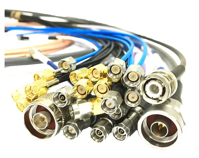
This process increases the hardness of the metal surface while retaining good abrasion, corrosion and discoloration resistance. Hard gold plating layers are extremely conductive and have excellent corrosion resistance, preventing oxidation and corrosion on the surface of the circuit board. In addition, hard gold plating provides good solderability and is suitable for circuit boards that require frequent maintenance and disassembly. It is often used in high-end electronic products, such as communication equipment and military equipment , which have excellent performance in terms of electrical performance and reliability.
Hard gold plating process is relatively complex and may be more expensive than soft gold. Although hard gold has higher hardness, it may be deformed when squeezed under external force, because most of it is hollow, so it is difficult to repair if it is deformed.
The difference between hard gold and soft gold is the composition of the last layer of gold plated on the gold plating, gold plating can choose to plating pure gold or alloy, because the hardness of pure gold is relatively soft, so it is also called “soft gold”. Because “gold” and “aluminum” can form a good alloy, so COB in the aluminum wire will be especially required to play the thickness of the layer of pure gold.
In addition, if you choose to plating gold-nickel alloy or gold-cobalt alloy, because the alloy will be harder than pure gold, so it is also called “hard gold”.
Plating procedures for soft and hard gold:
Soft gold: pickling → nickel plating → pure gold plating
Hard gold: Pickling → Electroless nickel plating → Pre-gold plating (flash gold) → Electroless nickel gold or gold-cobalt alloy plating
Hard gold plating differs from immersion gold in that its thickness can be varied by controlling the duration of the plating cycle, although typical minimum values for gold references are 30u “over 100u” nickel and 50u “over 100u” nickel for IPC Class 1 and IPC Class 3 respectively. ” nickel. Hard gold is generally not suitable for use in solderable areas due to its high cost and relatively poor solderability. the IPC considers the maximum thickness that can be soldered to be 17.8u”, so if this type of gold must be used for soldering, the recommended nominal thickness should be 5 to 10u”.
Advantages of using hard gold plating are: hard and durable surface, lead free, and long shelf life.
The disadvantages of using hard gold plating are: very expensive, requires additional processing in PCB production, more difficult than other surface treatments, and cannot be soldered above 17u”.
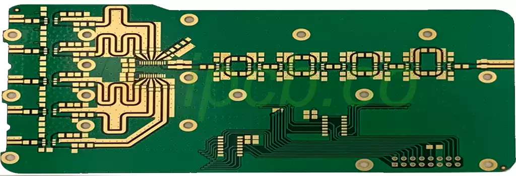
PCB hard gold plating technology is widely used in communications, computers, consumer electronics, automotive electronics and other fields. In electronic equipment working under extreme conditions such as high frequency, high speed and high temperature, this technology can significantly improve the performance and reliability of electronic components to meet the needs of complex and changing applications.
PCB hard gold plating technology as one of the key processes to enhance the performance of electronic components, in the field of electronics manufacturing plays an increasingly important role.