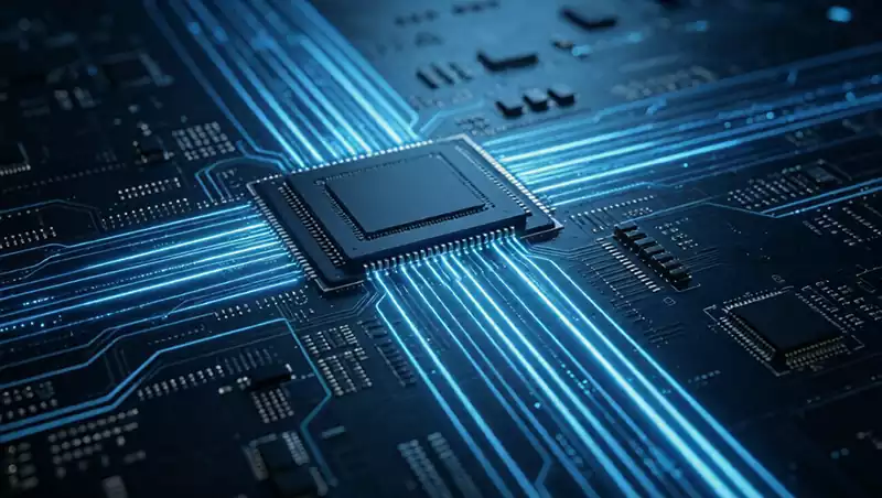
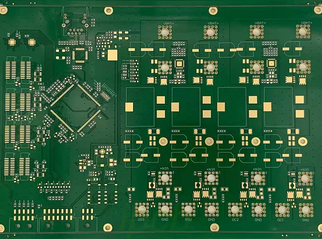
What is multilayer pcb? Multilayer board refers to more than three layers of conductive graphics layer and the insulating material between them in order to separate the laminated and the conductive graphics between them according to the requirements of the interconnection of the printed circuit board. It is electronic information technology to high-speed, multi-functional, high-capacity, small volume, thin, lightweight development of the direction of the product. Usually consists of multi-layer copper foil, insulating medium and connecting layer. Among them, the copper foil layer and the insulating medium form a “layer-to-layer” structure, while the connecting layer is used to connect each copper foil layer. In addition, multilayer boards include ears (VIA), which are vias from the top layer to the bottom layer and from the bottom layer to the top layer for electrical connections.
Before designing a multilayer PCB circuit board, the designer needs to first determine the board structure to be used based on the size of the circuit, board dimensions, and electromagnetic compatibility (EMC) requirements, that is, to decide whether to use a 4-layer, a 6-layer, or a higher number of layers. After determining the number of layers, it is then determined where the internal electrical layers will be placed and how the different signals will be distributed across these layers. This is the problem of choosing the layered structure of a multilayer PCB. Layer structure is an important factor affecting the EMC performance of the PCB board, but also an important means of suppressing electromagnetic interference.
How to make a multilayer pcb
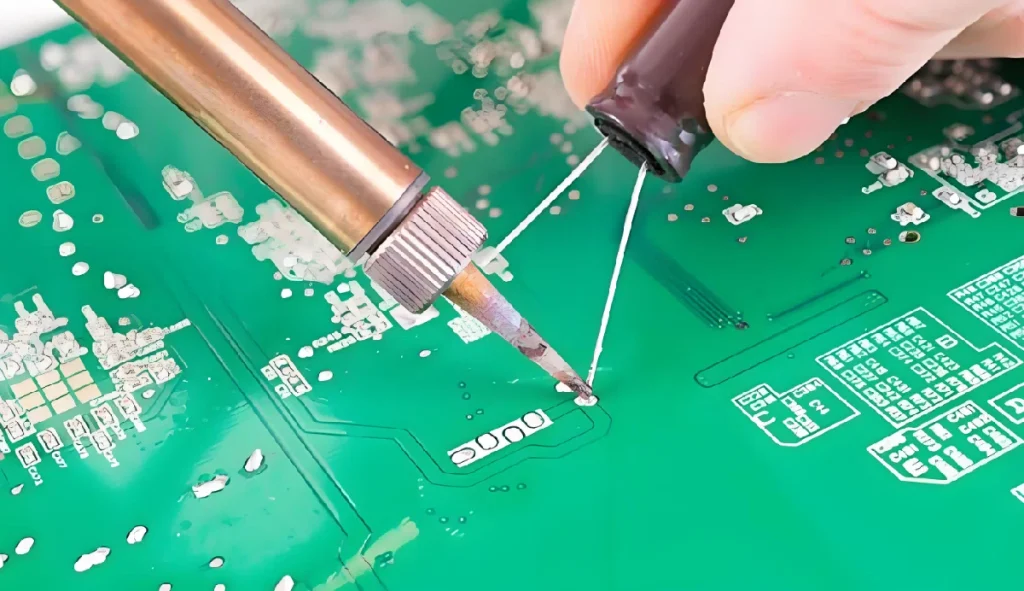
The manufacturing process of a multilayer circuit board includes the main steps of lamination, film forming, drilling, copper plating and graphic drawing.
First of all, lamination is one of the key steps in multilayer pcb manufacturing.In this process, engineers need to convert the designed circuit diagram into an actual circuit layout. This is usually accomplished through methods such as photolithography and electroplating. Photolithography is a method of projecting a circuit diagram directly onto a photosensitive material, which is then chemically cured to form a conductive film. Electroplating, on the other hand, is a method of depositing a metal or other conductive material onto the surface of the photosensitive material, thereby forming a metallic layer with the desired conductive properties.
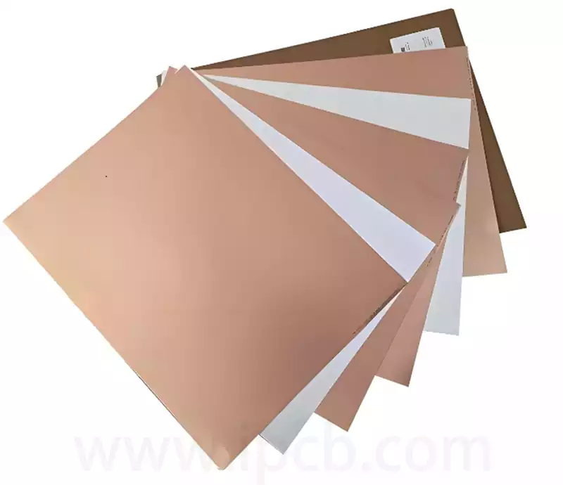
Next, the film formation process begins. At this stage, engineers need to select suitable film materials and coat them onto the photosensitive material.These film materials can be polyester film, fiberglass cloth, etc. The coating process usually involves techniques such as hot pressing and vacuum vaporization to ensure that the film adheres evenly to the photosensitive material.
Once the film is complete, the step of adding drilling can take place. This process involves drilling holes in the circuit board so that components can be mounted in subsequent steps.The addition drilling process can be performed using equipment such as mechanical, chemical or laser drilling machines. Depending on the design and requirements of the circuit board, different types of drills can be selected for the process.
The next step is the copper immersion plating step. In this process, engineers need to form a copper conductive layer on the circuit board. This is usually achieved through methods such as chemical copper plating or thermal copper plating. Chemical copper plating involves adding copper salts to a solution and then electrolytically depositing copper ions onto the board. Thermal copper plating is done by heating the board at high temperatures, causing a chemical reaction with the copper salts to form a copper conductive layer.
Finally, there is the graphics drawing step. In this stage, engineers need to use computer-aided design (CAD) software to create a design file of the circuit board and convert it into an actual board layout. The designed graphics are then transferred to the circuit board through processes such as etching and depaneling. Once this step is completed, the multilayer pcb board completes the manufacturing process.
Layer selection and stacking principles
Determine the multilayer circuit board structure needs to consider more factors. From the wiring aspect, the more layers the more favorable to the wiring, but the cost and difficulty of the board will also increase. For manufacturers, the symmetry of the layer structure is the focus of attention when manufacturing PCBs, so the choice of the number of layers needs to take into account the needs of all aspects in order to achieve the best balance.
For experienced designers, after completing the pre-layout of components, they will focus on analyzing the wiring bottlenecks of the PCB. Combined with other EDA tools to analyze the board’s wiring density; and then integrated with special wiring requirements of the signal lines such as differential lines, sensitive signal lines, etc., the number and type to determine the number of layers of the signal layer; and then according to the type of power supply, isolation and anti-jamming requirements to determine the number of layers of the internal electrical layer. In this way, the number of layers of the entire circuit board is basically determined.
After determining the number of layers of the circuit board, the next step is to reasonably arrange the placement order of the various layers of the circuit. In this step, the factors to be considered are mainly the following two points:
(1) The distribution of special signal layers.
(2) Distribution of power and ground layers.
If the number of layers of the circuit board, the more layers, special signal layer, ground layer and power supply layer of the arrangement of the combination of the more varieties, how to determine which combination is optimal is also more difficult, but the general principles are as follows:
(1) The signal layer should be adjacent to an internal power layer (internal power/ground layer), utilizing the large copper film of the internal power layer to provide shielding for the signal layer.
(2) The internal power and ground layers should be tightly coupled, i.e.,the dielectric thickness between the internal power and ground layers should take on a smaller value to increase the capacitance between the power and ground layers and increase the resonant frequency. The dielectric thickness between the internal power and ground layers can be set in Protel’s Layer Stack Manager. Select [Design]/[Layer Stack Manager…] command, the system pops up the Layer Stack Manager dialog box, double-click on the Prepreg text with the mouse, pop-up dialog box shown in Figure 11-1, you can change the thickness of the insulation layer in the Thickness option of the dialog box. If the potential difference between power and ground is not large, you can use a smaller insulation layer thickness, such as 5 mil (0.127 mm).
(3) The high-speed signaling layer in the circuit should be a signaling intermediate layer and be sandwiched between the two inner layers. In this way, the copper film of the two inner layers can provide electromagnetic shielding for high-speed signal transmission,and also effectively limit the radiation of high-speed signals between the two inner layers, without causing interference to the outside world.
(4) Avoid two signal layers directly adjacent to each other. It is easy to introduce crosstalk between adjacent signal layers, which can lead to circuit failure. Adding a ground plane between two signal layers can effectively avoid crosstalk.
(5) Multiple grounded internal electrical layers can effectively reduce ground impedance. For example, the use of separate ground planes for the A signal layer and the B signal layer can effectively reduce common mode interference.
(6) The symmetry of the layer structure is taken into account.
Advantages of multilayer pcb board
High space utilization. Because multilayer circuit board can be arranged on the same board multiple circuit layers, so you can greatly reduce the size of the circuit board, making electronic products more lightweight and portable. At the same time, it can also reduce the length of the signal line, reduce the signal transmission delay, improve the working speed and stability of the circuit.
Good anti-interference performance.The insulation between different layers can effectively isolate the signal lines and power lines, reducing the interference between each other.This is especially important for high-frequency circuits and analog circuits to provide more stable and reliable signal transmission.
Helps improve the thermal performance of the circuit. Since multilayer circuit boards have a large heat dissipation area, heat dissipation can be improved by adding heat dissipation layers or holes. This is especially important for electronic devices with high power consumption, which can effectively reduce the temperature and extend the service life of electronic products.
Disadvantages of multilayer printed circuit board
Higher manufacturing costs. Compared with single-layer boards, multilayer boards require more processes and materials, so the manufacturing cost will be relatively high.
Higher design complexity. Since multilayer circuit boards involve wiring and connections between multiple circuit layers, the design process is relatively complex and requires more specialized skills and experience.
As an important product of the development of modern electronic information technology, multilayer pcb boards provide strong support for the thinness, high speed and multifunctionality of electronic products with their unique design and manufacturing methods.It will continue to play an important role in the electronics industry as technology continues to advance and the market continues to demand.