Printed Circuit Boards (PCBs) form the backbone of modern electronic devices, serving as the platform that connects and supports various electronic components. An empty PCB board, devoid of its intricate web of components, represents the starting point of electronic innovation. This article delves into the significance, types, manufacturing processes, applications, and future trends of empty PCB boards.
The Significance of Empty PCB Boards
Empty PCB boards are essential to electronic design and manufacturing. They serve as the foundational canvas upon which electronic components are mounted and interconnected. The layout of an empty PCB board determines the efficiency, reliability, and performance of the final electronic device. Engineers and designers use sophisticated software tools to plan and design the intricate pathways and connections that will be etched onto the PCB.
In the world of electronics, the importance of the empty PCB board cannot be overstated. It is akin to the foundation of a building; without a solid and well-planned base, the entire structure could be compromised. The precision and detail involved in designing the PCB layout directly affect the functionality and durability of the electronic device. A well-designed PCB ensures optimal signal integrity, minimizes electromagnetic interference, and enhances thermal management, all of which are critical for the device’s overall performance.
Moreover, the empty PCB board is a versatile and customizable platform. Depending on the application, it can be designed to meet specific requirements such as size, shape, and electrical performance. This adaptability makes PCBs suitable for a wide range of industries, from consumer electronics to aerospace and defense.
Types of PCB Boards
PCBs come in various types, each suited to different applications and requirements. The most common types include single-sided, double-sided, and multi-layer PCBs.
Single-sided PCBs have copper traces on only one side of the board, making them simple and cost-effective. They are typically used in low-complexity devices such as calculators and power supplies.
Double-sided PCBs feature copper traces on both sides of the board, allowing for more complex circuitry and increased component density. They are commonly found in applications such as automotive dashboards and industrial control systems.
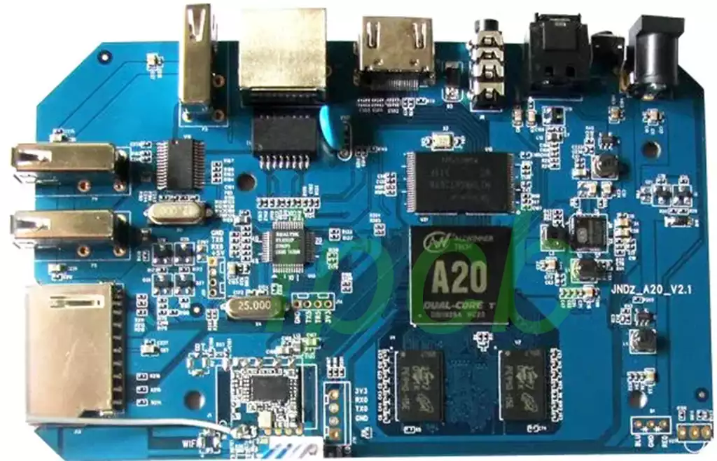
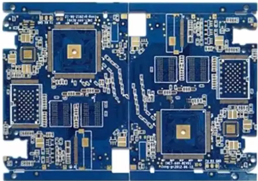
Multi-layer PCBs consist of multiple layers of copper traces separated by insulating layers. This design allows for even more complex circuitry and higher component density. Multi-layer PCBs are used in advanced applications like smartphones, computers, and high-frequency communication devices.
In addition to these standard types, there are also specialized PCBs designed for specific purposes. For instance, rigid PCBs are made from solid, inflexible materials and are commonly used in applications where the board needs to maintain a fixed shape. Flexible PCBs, on the other hand, are made from flexible materials that can bend and twist, making them ideal for wearable devices and other applications where space is limited.
Rigid-flex PCBs combine the advantages of both rigid and flexible boards. They consist of multiple layers of rigid and flexible PCBs laminated together, allowing for greater design flexibility and improved reliability. These hybrid boards are often used in aerospace, medical, and military applications, where performance and durability are paramount.
Another type is the high-frequency PCB, which is designed to operate at high frequencies with minimal signal loss. These PCBs are made from specialized materials that have low dielectric loss and are used in applications such as satellite communication, radar systems, and advanced telecommunications.
Manufacturing Processes
The manufacturing of empty PCB boards involves several intricate steps, each critical to ensuring the quality and reliability of the final product.
Design: The process begins with designing the PCB layout using specialized software. Engineers create a schematic diagram that outlines the placement of components and the connections between them. This design phase is crucial as it determines the electrical performance and physical layout of the PCB.
Material Selection: The choice of materials is crucial to the performance of the PCB. Common materials include FR4, a composite material made of woven fiberglass and epoxy resin, and more advanced materials like polyimide for high-temperature applications. The material selected must have the appropriate electrical, thermal, and mechanical properties to meet the specific requirements of the application.
Laminating: The base material is laminated with a thin layer of copper foil on one or both sides. This copper layer will be etched to create the desired circuit patterns. The lamination process involves applying heat and pressure to bond the copper foil to the substrate material.
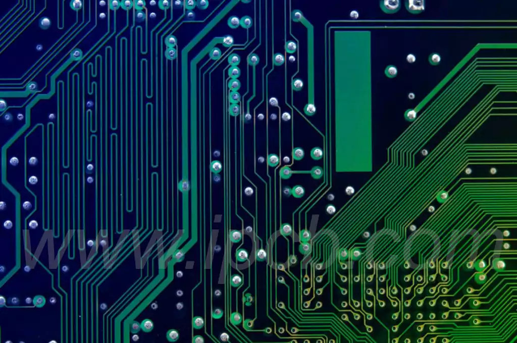
Etching: In this step, the unwanted copper is removed, leaving behind the copper traces that form the circuit. Chemical etching or more advanced techniques like laser etching are used to achieve precise results. The etching process must be carefully controlled to ensure that the copper traces are accurately formed and free of defects.
Drilling: Holes are drilled into the board to allow for the placement of through-hole components and to create vias that connect different layers of multi-layer PCBs. The drilling process must be precise to ensure that the holes are accurately placed and sized.
Plating: The drilled holes are plated with copper to establish electrical connections between the different layers of the PCB. This step is critical for multi-layer PCBs, where reliable inter-layer connections are essential for the board’s functionality.
Solder Mask and Silkscreen: A solder mask is applied to protect the copper traces and prevent short circuits during soldering. A silkscreen layer is added to provide component labels and other markings. The solder mask and silkscreen layers enhance the durability and usability of the PCB.
Testing: The finished PCB undergoes rigorous testing to ensure that it meets design specifications and is free from defects. Electrical testing, visual inspection, and automated optical inspection (AOI) are commonly used to verify the quality of the PCB.
In recent years, advancements in PCB manufacturing technology have led to more efficient and precise processes. For example, direct imaging technology allows for higher resolution and accuracy in the etching process, enabling the production of finer and more complex circuit patterns. Additionally, advancements in materials science have led to the development of high-performance PCB materials that offer improved thermal and electrical properties.
Applications of Empty PCB Boards
Empty PCB boards are the building blocks of a vast array of electronic devices, each serving a unique purpose in various industries.
Consumer Electronics: From smartphones and tablets to televisions and gaming consoles, PCBs are integral to the operation of modern consumer electronics. Their compact design and high component density enable the creation of powerful and feature-rich devices. The continuous miniaturization of consumer electronics has driven the demand for smaller, more efficient PCBs that can accommodate more components in a limited space.
Automotive: The automotive industry relies heavily on PCBs for various applications, including engine control units, infotainment systems, and advanced driver-assistance systems (ADAS). PCBs in automotive applications must withstand harsh environments and high temperatures. As vehicles become more advanced and incorporate more electronic systems, the demand for reliable and high-performance PCBs continues to grow.
Medical Devices: PCBs play a critical role in medical devices such as pacemakers, MRI machines, and diagnostic equipment. Reliability and precision are paramount in medical applications, necessitating stringent quality control measures during PCB manufacturing. The increasing adoption of wearable medical devices and remote monitoring systems has also driven the demand for specialized PCBs that can operate reliably in medical environments.
Industrial Equipment: In industrial settings, PCBs are used in machinery, control systems, and automation equipment. They must endure demanding conditions and provide reliable performance to ensure the smooth operation of industrial processes. The rise of Industry 4.0 and the increasing use of IoT devices in industrial applications have further increased the demand for advanced PCBs that can support complex and interconnected systems.
Aerospace and Defense: PCBs used in aerospace and defense applications must meet rigorous standards for performance, reliability, and durability. They are found in aircraft avionics, satellite systems, and military communication devices. The critical nature of aerospace and defense applications requires PCBs that can operate reliably under extreme conditions, including high temperatures, vibration, and radiation.
Telecommunications: The telecommunications industry relies on PCBs for a wide range of applications, including base stations, routers, and network infrastructure equipment. High-frequency PCBs are essential for supporting the high-speed data transmission required in modern communication systems. The deployment of 5G technology and the increasing demand for high-speed internet have driven the need for advanced PCBs that can support higher frequencies and greater data throughput.
Energy and Power: PCBs are used in energy and power applications, including renewable energy systems, power converters, and smart grid technology. These PCBs must be designed to handle high power levels and provide reliable performance in demanding environments. The transition to renewable energy sources and the increasing adoption of electric vehicles have created new opportunities for PCB applications in the energy sector.
Future Trends in PCB Technology
As technology continues to advance, the field of PCB design and manufacturing is poised for significant innovation. Several trends are shaping the future of empty PCB boards.
Miniaturization: The demand for smaller, more powerful electronic devices is driving the need for miniaturized PCBs. Advances in materials and manufacturing techniques are enabling the production of PCBs with higher component densities and reduced footprints. The development of advanced packaging technologies, such as system-in-package (SiP) and chip-on-board (COB), allows for even greater integration of components on a single PCB.
Flexible and Rigid-Flex PCBs: Flexible PCBs, made from materials that can bend and twist, are gaining popularity in applications where traditional rigid PCBs are impractical. Rigid-flex PCBs combine the advantages of both rigid and flexible boards, offering enhanced design flexibility. The increasing demand for wearable devices, flexible displays, and other innovative applications has driven the growth of the flexible and rigid-flex PCB market.
High-Frequency PCBs: With the rise of 5G technology and high-frequency communication systems, PCBs must operate at higher frequencies with minimal signal loss. Specialized materials and design techniques are being developed to meet these demands. The deployment of 5G networks and the increasing demand for high-speed data transmission have created new opportunities for high-frequency PCB applications.
Environmental Considerations: Sustainability is becoming increasingly important in PCB manufacturing. Efforts are being made to develop eco-friendly materials, reduce waste, and improve recycling processes for end-of-life PCBs. The adoption of green manufacturing practices, such as the use of lead-free solder and the reduction of hazardous substances, is becoming more widespread in the PCB industry.
Advanced Manufacturing Techniques: Emerging technologies such as additive manufacturing (3D printing) and laser direct structuring (LDS) are revolutionizing PCB production. These techniques offer greater design freedom, faster prototyping, and the potential for more complex and integrated PCB structures. The use of advanced manufacturing techniques also allows for the production of customized PCBs with unique shapes and features, opening up new possibilities for innovative applications.
Internet of Things (IoT): The proliferation of IoT devices has created a demand for specialized PCBs that can support the unique requirements of IoT applications. IoT devices often require PCBs with low power consumption, compact size, and wireless connectivity features. The development of PCBs tailored for IoT applications is a growing area of focus for the PCB industry.
Artificial Intelligence (AI) and Machine Learning: The integration of AI and machine learning technologies in electronic devices is driving the need for advanced PCBs that can support high-speed data processing and complex algorithms. The development of AI-enabled PCBs, which incorporate specialized hardware for AI processing, is an emerging trend in the PCB industry.
Wearable Technology: The increasing popularity of wearable technology, such as smartwatches, fitness trackers, and medical monitoring devices, has created a demand for flexible and miniaturized PCBs that can be integrated into small, portable devices. The development of advanced materials and manufacturing techniques is enabling the production of PCBs that can meet the unique requirements of wearable technology applications.
Conclusion
Empty PCB boards may appear simple at first glance, but they are the foundation upon which the entire world of electronics is built. Their design, manufacturing, and application encompass a vast and complex field that continues to evolve with technological advancements. As we look to the future, the innovations in PCB technology promise to drive further progress in electronic devices, making them smaller, more powerful, and more versatile than ever before.
The significance of empty PCB boards extends beyond their physical presence. They represent the starting point of electronic innovation, where ideas and concepts are transformed into tangible and functional devices. The continuous advancements in PCB technology and manufacturing processes are enabling the development of increasingly complex and high-performance electronic systems.
As the demand for more sophisticated and compact electronic devices grows, the role of empty PCB boards becomes even more critical. The ability to design and manufacture PCBs that can meet the stringent requirements of modern applications is essential for the continued progress of the electronics industry.
In conclusion, the empty PCB board is a vital component of electronic design and manufacturing. Its importance lies in its ability to provide a reliable and customizable platform for the development of a wide range of electronic devices. The ongoing advancements in PCB technology and the emergence of new trends are shaping the future of the industry, driving innovation and enabling the creation of next-generation electronic systems.
By understanding the significance, types, manufacturing processes, applications, and future trends of empty PCB boards, we gain a deeper appreciation for the complexity and intricacy involved in the world of electronic design. The empty PCB board may be just the starting point, but it is the foundation upon which the entire world of electronics is built, paving the way for future advancements and technological breakthroughs.