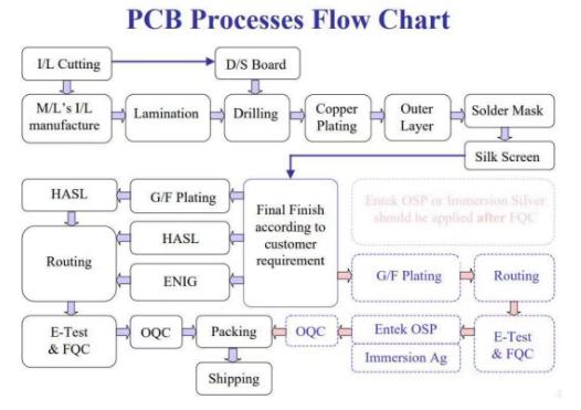
Printed Circuit Boards (PCBs) are the backbone of modern electronics, facilitating the interconnection and functionality of various electronic components. The PCB manufacturing process is a meticulous and technically demanding sequence of steps aimed at ensuring the reliability, performance, and durability of these critical components. This comprehensive guide explores in detail each stage of the PCB board manufacturing process, highlighting its technical intricacies, importance, and the advancements shaping the industry.
Introduction to PCB Board Manufacturing
Printed Circuit Boards (PCBs) are essential components used in nearly every electronic device, from smartphones to industrial machinery. These boards provide the mechanical support and electrical connections necessary for the proper functioning of electronic circuits. The manufacturing of PCBs involves a series of precise steps, each contributing to the overall quality and reliability of the final product.
Design and Layout Phase
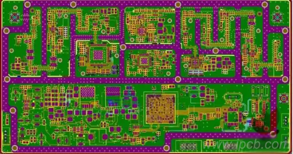
The journey of PCB manufacturing begins with the design and layout phase. Engineers and designers utilize specialized software tools to translate circuit schematics into physical designs. This phase is crucial as it determines the placement of components, the routing of electrical connections (traces), and the overall layout of the board. The goal is to optimize the design for functionality, efficiency, and manufacturability.
Material Selection for PCBs
Material selection is a critical aspect of PCB manufacturing, directly impacting performance, durability, and cost. The base material typically used for PCBs is a fiberglass-reinforced epoxy laminate known as FR-4. This material provides mechanical support and electrical insulation. Copper is the primary choice for conductive pathways due to its excellent electrical conductivity. Other materials, such as solder mask and silkscreen ink, are applied to protect copper traces from environmental factors and to provide labeling for component placement.
Inner Layer Processing: Imaging and Etching
Once the design is finalized, the manufacturing process moves to inner layer processing. This phase involves creating the core structure of the PCB. A thin layer of copper is laminated onto both sides of the FR-4 substrate. The next step is imaging, where a layer of photoresist material is applied to the copper surface. The board is then exposed to UV light through a photographic mask, which transfers the circuit pattern onto the photoresist.
After exposure, the board undergoes a development process that removes the unexposed photoresist, leaving behind the desired circuit pattern. Following this, the exposed copper areas not protected by the photoresist are etched away using chemical solutions. The remaining photoresist is then stripped off, leaving the copper traces that form the conductive pathways of the PCB.
Lamination Process
With the inner layers prepared, the PCB enters the lamination process. This involves bonding together multiple layers of substrate and copper foil to create a single, multi-layered board. Pre-preg layers, which are sheets of fiberglass impregnated with epoxy resin, are placed between the copper-clad layers. The entire stack is then pressed together under heat and pressure in a lamination press.
The heat activates the resin in the pre-preg layers, causing them to bond securely with the copper layers. This process creates a solid, unified structure with insulated conductive pathways between layers. Lamination not only ensures electrical connectivity but also enhances the mechanical strength and rigidity of the PCB, making it capable of withstanding environmental stresses and mechanical loads.
Drilling of PCBs
Once laminated, the next step in the pcb manufacturing process is drilling. Holes, known as vias, are drilled into the PCB to establish electrical connections between different layers of the board. These vias also accommodate the leads of electronic components that will be mounted on the PCB during assembly. Drilling is a precision operation that requires high-accuracy machines equipped with carbide drills.
The drill bits must accurately position and size the holes according to the design specifications. After drilling, the PCB undergoes a thorough cleaning process to remove any residual debris or contaminants left from the drilling operation. This cleaning step is crucial to ensure the integrity of the vias and the quality of subsequent manufacturing processes.
Copper Plating and Surface Finishing
Following drilling, the PCB moves to the copper plating stage. Copper plating is applied to the walls of the vias and to the exposed copper surfaces on the PCB. Initially, a thin layer of copper is deposited using a chemical deposition process, which ensures that the vias are fully coated and the exposed copper areas are covered uniformly.
Electroplating is then used to build up the thickness of the copper layer to the required level, typically around 25 to 35 microns. This thicker layer of copper enhances the conductivity of the PCB and provides mechanical strength to the conductive pathways. Once the electroplating process is complete, the excess copper is etched away from the non-circuit areas using chemical solutions, leaving behind the desired copper traces and vias.
Surface finishing follows copper plating and involves applying a protective layer to the exposed copper surfaces of the PCB. Common surface finishes include:
- HASL (Hot Air Solder Leveling): Involves dipping the PCB into molten solder and then using hot air to remove excess solder, leaving a flat, solder-coated surface.
- ENIG (Electroless Nickel Immersion Gold): Provides excellent corrosion resistance and solderability by depositing a thin layer of gold over a layer of nickel on the PCB surface.
- OSP (Organic Solderability Preservative): Applies a thin organic layer that protects the copper surface from oxidation and facilitates soldering during component assembly.
The choice of surface finish depends on factors such as cost, solderability, environmental resistance, and the specific requirements of the application.
Outer Layer Imaging and Etching
After surface finishing, the PCB undergoes outer layer imaging and etching processes. Similar to the inner layer process, a photoresist material is applied to the outer layer of copper. The PCB is then exposed to UV light through a photographic mask, which transfers the circuit pattern onto the photoresist. After exposure, the board undergoes a development process to remove the unexposed photoresist, leaving behind the desired circuit pattern on the outer layer.
The exposed copper areas are then etched away using chemical solutions, leaving behind the final copper traces that form the conductive pathways on the outer layer of the PCB. Advanced techniques such as plasma etching may be used for finer traces and more complex designs, ensuring precision and accuracy in the etching process.
Solder Mask Application
With the circuit patterns defined, the next step is the application of solder mask. Solder mask is a protective layer applied to the PCB to insulate the copper traces and prevent solder bridges during component assembly. The solder mask also protects the PCB from environmental factors such as dust, moisture, and chemical contaminants.
The solder mask material is applied in liquid form and then cured using UV light to harden and solidify the layer. After curing, openings (called “exposes”) are created in the solder mask over the solder pads and vias where electrical connections will be made during component soldering. The color of the solder mask, typically green, helps to distinguish between different PCBs and aids in the visual inspection of the board.
Silkscreen Printing
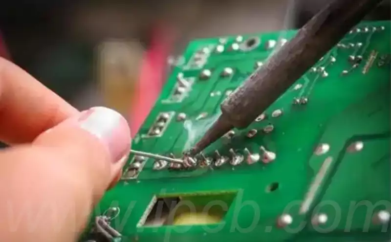
Silkscreen printing is the final step in the PCB manufacturing process before assembly. This process involves applying a layer of non-conductive ink onto the surface of the PCB. The ink is applied through a silkscreen mesh that transfers the desired design onto the PCB surface. Silkscreen printing is used to apply component designators, logos, part numbers, and other identifying information directly onto the PCB.
This information aids in the assembly and identification of components during the manufacturing process and helps technicians and engineers to troubleshoot and maintain the PCB throughout its operational life. Automated silkscreen printing systems ensure consistent and accurate application of ink across multiple PCBs, maintaining high-quality standards and minimizing production errors.
Electrical Testing and Quality Control
Once the PCB has been fully manufactured, it undergoes rigorous electrical testing and quality control procedures to ensure that it meets the required specifications and performance standards. Automated test equipment (ATE) is used to perform a series of tests, including:
- Continuity Testing: Checks for the presence of electrical connections between designated points on the PCB.
- Insulation Resistance Testing: Measures the resistance between conductive pathways to ensure there are no unintended connections or shorts.
- Functional Testing: Evaluates the operational performance of the PCB under simulated operating conditions, verifying that all components function correctly and that the board meets its intended functionality.
These tests are essential for identifying any manufacturing defects, such as open circuits, short circuits, or incorrect component placements. Any detected defects are documented, and corrective actions are taken to address them before the PCB proceeds to the next stage of production or assembly.
Final Inspection and Packaging
After passing electrical testing and quality control, the final step is inspection and packaging. Visual inspection is conducted to check for any cosmetic defects, such as scratches, smudges, or misaligned components. Automated optical inspection (AOI) systems may also be used to perform detailed inspections of the PCB surface, ensuring that all solder joints are properly formed and that there are no defects in the solder mask or silkscreen printing.
For multi-layer PCBs, X-ray inspection may be employed to verify the integrity of internal vias and connections that are not visible on the surface. Once inspected and approved, the PCBs are carefully packaged using anti-static materials to protect them from electrostatic discharge (ESD) during shipping and handling. Proper packaging also prevents physical damage and ensures that the PCBs arrive at their destination in pristine condition, ready for assembly into electronic devices.
Conclusion
The PCB board manufacturing process is a complex and highly structured sequence of steps that ensures the creation of reliable, high-performance circuit boards for use in various electronic applications. Each stage of the process—from design and material selection to final