Introduction to Bare PCB Boards
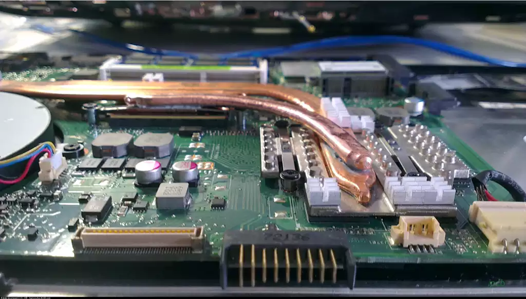
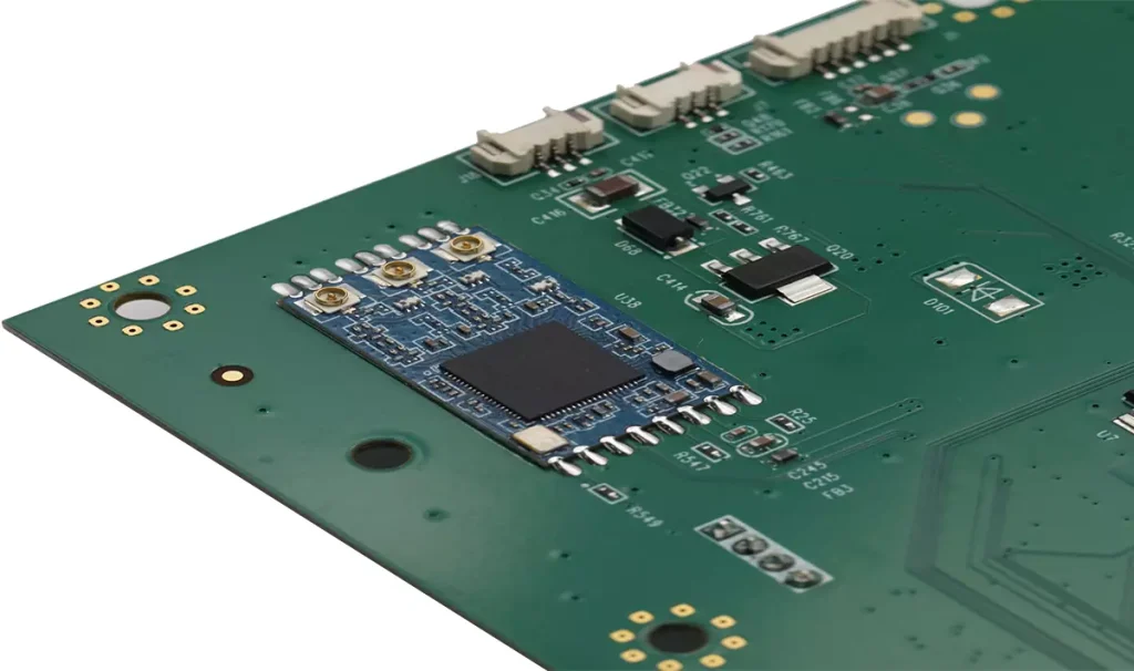
A Bare PCB Board, also known as a bare printed circuit board, is the foundational platform for assembling electronic components to create a functional PCB assembly. This essential component in electronics manufacturing serves as the backbone for electronic circuits, providing both the physical structure and electrical connectivity needed to support and interconnect various electronic components.
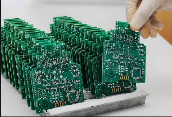
Structure of Bare PCB Boards
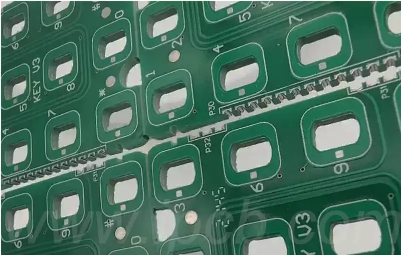
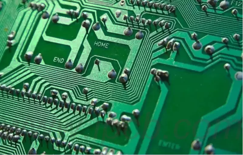
Bare PCB boards are typically made from a non-conductive substrate material, such as fiberglass reinforced epoxy resin (FR-4), which provides the board with its rigidity and electrical insulation properties. The surface of the board is coated with a thin layer of conductive material, usually copper, which forms the electrical pathways, or traces, that connect different components. These copper traces are created through a process known as photolithography, where a photoresist material is applied to the copper surface, exposed to light through a mask, and then developed to reveal the desired circuit pattern.
Types of Bare PCB Boards
Bare PCB boards come in various types, each designed to meet specific requirements and applications. The most common types include:
- Single-Sided PCBs: These boards have copper traces on one side of the substrate only. They are the simplest and most cost-effective type of PCB, suitable for low-density designs and less complex circuits.
- Double-Sided PCBs: These boards have copper traces on both sides of the substrate, allowing for more complex and higher-density designs. They are commonly used in consumer electronics, industrial equipment, and automotive applications.
- Multi-Layer PCBs: These boards consist of multiple layers of substrate and copper traces, laminated together to form a single board. They are used in highly complex and dense designs, such as computer motherboards, smartphones, and high-performance computing devices.
- Flexible PCBs: Made from flexible materials like polyimide, these boards can bend and twist to fit into compact or irregularly shaped spaces. They are commonly used in wearable electronics, medical devices, and flexible displays.
- Rigid-Flex PCBs: These boards combine the characteristics of both rigid and flexible PCBs, providing the benefits of both types in a single design. They are used in applications requiring both rigidity and flexibility, such as aerospace and military equipment.
Manufacturing Process of Bare PCB Boards
The manufacturing process of bare PCB boards involves several key steps, each critical to ensuring the quality and functionality of the final product. These steps include:
- Design and Layout: The first step is to create a detailed design and layout of the PCB using specialized software tools. This design includes the placement of components, the routing of traces, and the definition of the board’s layers.
- Material Preparation: The substrate material, usually FR-4, is cut to the required size and cleaned to remove any contaminants.
- Copper Cladding: A thin layer of copper is laminated onto the surface of the substrate material. This copper layer will be used to create the circuit traces.
- Photoresist Application: A photoresist material is applied to the copper surface. This material is sensitive to light and will be used to create the circuit pattern.
- Exposure and Development: The photoresist-coated board is exposed to light through a mask that defines the desired circuit pattern. The exposed areas of the photoresist harden, while the unexposed areas remain soft and can be removed.
- Etching: The board is then subjected to a chemical etching process that removes the unprotected copper, leaving behind the desired circuit traces.
- Drilling: Holes are drilled in the board to create vias and mounting points for components. These holes are then plated with copper to ensure electrical connectivity.
- Solder Mask Application: A solder mask is applied to the board to protect the copper traces and prevent solder bridges during component assembly. The solder mask also provides insulation and mechanical protection.
- Silkscreen Printing: A silkscreen layer is printed on the board to add labels, component outlines, and other markings that aid in assembly and troubleshooting.
- Final Inspection and Testing: The finished board undergoes a series of inspections and tests to ensure it meets quality and performance standards. This includes visual inspection, electrical testing, and functional testing.
Quality Control in Bare PCB Board Manufacturing
Quality control is a crucial aspect of bare PCB board manufacturing. Ensuring that each board meets stringent quality standards is essential to the reliability and performance of the final electronic products. Here are some key quality control measures:
- Visual Inspection: Visual inspections are performed at various stages of the manufacturing process to detect any visible defects, such as scratches, misalignments, or incomplete etching.
- Electrical Testing: Electrical tests, including continuity and isolation tests, are conducted to verify that the copper traces and vias are correctly formed and that there are no short circuits or open circuits.
- X-ray Inspection: X-ray inspection is used to examine the internal structure of multi-layer PCBs, ensuring that the layers are properly aligned and that there are no hidden defects such as voids or misregistrations.
- Solderability Testing: This test evaluates the solderability of the board’s surface, ensuring that components can be reliably soldered without issues such as poor wetting or dewetting.
- Environmental Testing: Environmental tests simulate various conditions that the PCB might encounter during its lifecycle, such as temperature cycling, humidity exposure, and thermal shock, to ensure the board’s durability and reliability.
Applications of Bare PCB Boards
Bare PCB boards are used in a wide range of applications across various industries. Some of the most common applications include:
- Consumer Electronics: Bare PCB boards are found in virtually all consumer electronic devices, such as smartphones, tablets, laptops, televisions, and gaming consoles. They provide the essential platform for assembling and interconnecting the various electronic components that make these devices function.
- Industrial Equipment: In industrial settings, bare PCB boards are used in machinery control systems, automation equipment, sensors, and other electronic devices. They enable the precise control and monitoring of industrial processes, enhancing efficiency and productivity.
- Automotive Electronics: Modern vehicles rely on bare PCB boards for various electronic systems, including engine control units, infotainment systems, navigation systems, and advanced driver assistance systems (ADAS). These boards ensure reliable and efficient operation of the vehicle’s electronic systems.
- Medical Devices: In the medical field, bare PCB boards are used in diagnostic equipment, monitoring devices, and therapeutic devices. They enable the accurate and reliable operation of medical electronics, contributing to improved patient care and outcomes.
- Telecommunications: Bare PCB boards are essential components in telecommunications equipment, such as routers, switches, modems, and base stations. They provide the necessary infrastructure for transmitting and receiving data, enabling communication networks to function effectively.
- Aerospace and Defense: In aerospace and defense applications, bare PCB boards are used in avionics, radar systems, communication systems, and other critical electronic systems. They ensure the reliable and robust performance of these systems in demanding environments.
Advances in Bare PCB Board Technology
As technology continues to advance, so does the development of bare PCB boards. These advancements aim to address the challenges and meet the demands of modern electronic devices and applications. Some notable trends and innovations include:
- High-Density Interconnect (HDI) PCBs: HDI PCBs feature finer traces and spaces, smaller vias, and higher layer counts, enabling more complex and compact designs. They are increasingly used in smartphones, tablets, and other portable devices.
- Embedded Components: Embedding passive and active components within the PCB substrate itself can reduce the overall size and improve the performance of electronic devices. This approach is particularly beneficial for high-frequency applications and space-constrained designs.
- Advanced Materials: New materials, such as high-frequency laminates and thermally conductive substrates, are being developed to meet the performance requirements of high-speed and high-power applications.
- Flexible and Stretchable PCBs: Flexible PCBs are evolving to become more durable and capable of withstanding extreme bending and stretching. These advancements open up new possibilities for wearable electronics, medical implants, and other innovative applications.
- Environmental Sustainability: There is a growing focus on developing eco-friendly PCB manufacturing processes and materials. This includes the use of lead-free solder, recyclable substrates, and reducing the environmental impact of chemical processes.
Conclusion
Bare PCB boards are fundamental components in the electronics industry, serving as the essential platform for assembling and interconnecting electronic components. Understanding their structure, types, manufacturing process, and applications is crucial for anyone involved in electronics design and manufacturing. As technology continues to evolve, the development of advanced PCB designs and materials will play a key role in enabling the next generation of electronic devices and systems. The ongoing advancements in PCB technology, coupled with stringent quality control measures, ensure that bare PCB boards will continue to meet the growing demands of various industries, driving innovation and progress in the field of electronics.