Buried capacitance pcb is a common technique used in PCB design to improve the performance of a system by embedding capacitors inside the PCB board.PCB buried capacitors are capacitors made inside the PCB board, and the capacitors made in this way are called buried capacitors. The embedded capacitors can be ceramic, tantalum or polymer capacitors, etc. Depending on the application scenario, different types of capacitors can be selected!
- Discrete Capacitors
In the pcb design according to the size of the capacitance value required to calculate the graphical area of the capacitor, and then in the use of the power supply layer in the similar flower pads connected to the OK. - Common plane capacitance
No need to do special treatment in pcb design.
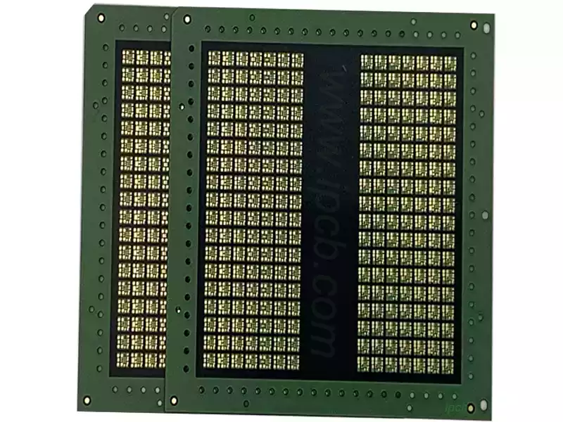
PCB buried capacitance process detailed steps:
- Make the internal layer:
In the production of PCB boards, in addition to conventional layers (such as the outer layer, the inner layer), but also need to make a separate internal layer dedicated to buried capacitance. These internal layers will contain areas for burying resistors and capacitors. The production of internal layers usually use the same technology as conventional PCB manufacturing, such as plating, etching, etc.. - Capacitor Encapsulation:
Capacitors are packaged in a special form in the buried capacitance process in order to be embedded in the internal layers of the PCB. These packages are usually thinned to accommodate the thickness of the circuit board and have good thermal conductivity. - Embedded resistors/capacitors:
The buried capacitance process is accomplished by embedding resistors and capacitors into the internal layers of the PCB board during the fabrication of the internal layers. This can be accomplished in a variety of ways, such as using special pressing techniques to embed resistors and capacitors between the inner layers, or using laser technology to etch cavities in the inner layers and then fill them with capacitors. - Connection layer:
After completing the inner layer of the buried capacitance, it is connected to other conventional layers (e.g., the outer layer). This can be achieved by conventional PCB manufacturing techniques (e.g. lamination, drilling, etc.).
Addition Process Considerations
- Due to the thin material, the patchwork is easy to be broken, should pay attention to the patchwork spacing wide and narrow staggered.
- BC16T material, if you need to play laser holes, you need to turn down the laser, otherwise the holes will be large.
- Etching graphics on one side, and it is best to use the leader board.
The role of buried capacitors pcb
- Improve the stability of the system: buried capacitance can effectively reduce external interference, improve the stability of the system
- Reduce volume: By embedding capacitors inside the PCB substrate, it can save space and reduce the volume of the whole system.
- Reduce cost: Embedded capacitors can reduce the connection of external capacitors and lower the cost.
- Improve signal transmission speed: Embedded capacitors can reduce the loss in the signal transmission process and improve the transmission speed.
Buried capacitance pcb technology has been widely used in smart phones, tablet PCs, wearable devices, servers, high-performance computing and other fields. The advantages are especially obvious in portable devices and data center servers that have strict requirements for size, weight, and power consumption. In the future, with the continuous progress of materials science, manufacturing process, buried capacitance circuit board technology is expected to further expand to automotive electronics, aerospace, medical electronics and other high-end fields, to promote the transformation and upgrading of the entire electronics industry.
Buried capacitor pcb technology with its excellent performance enhancement and miniaturization advantages, is profoundly changing the design pattern of electronic products, and will continue to promote the innovative development of the electronics industry in the future.