Horizontal plating technology is a new plating method developed on the basis of vertical plating technology. The key to horizontal plating is to improve the fluidity and dispersion of the plating solution by improving the plating system, so as to realize a more uniform and efficient plating effect.
Horizontal plating and vertical plating have the same methods and principles. They must have a cathode and anode. When energized, an electrode reaction occurs that ionizes the main components of the electrolyte, causing charged positive ions to move to the negative phase of the electrode reaction zone; and charged negative ions to move to the positive phase of the electrode reaction zone, resulting in the deposition of a metal coating and gas emissions.
Because the process of metal deposition at the cathode is divided into three steps: the hydrated ions of the metal diffuse into the cathode; the second step is that when the hydrated ions of the metal pass through the bilayer, they are gradually dehydrated and adsorbed on the surface of the cathode; and the third step is that the metal ions adsorbed on the surface of the cathode accept electrons and enter the metal lattice. The layer is smaller than the Helmholtz outer layer due to electrostatic forces and is subject to thermal motion. The cations are not arranged as closely and neatly as in the Helmholtz outer layer. This layer is called the diffusion layer. The thickness of the diffusion layer is inversely proportional to the flow rate of the plating solution. That is, the faster the flow rate of the plating solution, the thinner and thicker the diffusion layer. Usually, the thickness of the diffusion layer is about 5-50 microns. The layer of plating solution that arrives by convection away from the cathode is called the main plating solution. This is because convection of the solution affects the uniformity of the concentration of the plating solution. Copper ions in the diffusion layer are transported to the Helmholtz outer layer by diffusion and ion migration. Copper ions in the main plating solution are transported to the cathode surface by convection and ion migration. During horizontal plating, copper ions in the plating solution are transported to the vicinity of the cathode in three ways to form a double electric layer.
The process of metal deposition at the cathode is divided into three steps: the first step is the diffusion of the hydrated ions of the metal to the cathode; the second step is the gradual dehydration of the hydrated ions of the metal as they pass through the double electric layer and are adsorbed on the surface of the cathode; and the third step is the acceptance of the electrons by the metal ions adsorbed on the surface of the cathode and their entry into the metal lattice.
The key to the pcb plating is how to ensure the uniformity of the thickness of the copper layer on both sides of the substrate and the inner wall of the conduction holes. To get the uniformity of the thickness of the plating layer, it is necessary to ensure that the two sides of the printed circuit board and through-hole plating liquid flow rate should be fast and consistent, in order to obtain a thin and uniform diffusion layer. To achieve a thin and uniform diffusion layer.
On the current structure of the horizontal plating system,although the system installed many nozzles, can be plating liquid fast vertical spray to the printed board to accelerate the flow rate of plating liquid in the through-hole,resulting in the flow rate of plating liquid is very fast, in the substrate on the bottom and through-hole formation of vortex, so that the diffusion of the layer is reduced and more uniform.However,usually when the plating solution suddenly flows into the narrow through-hole,the plating solution at the entrance of the through-hole will also have the phenomenon of reverse reflux,coupled with the influence of the primary current distribution,the evolution of the entrance to the hole part of the plating often results in the entrance of the hole, due to the tip of the effect of the thickness of the copper layer caused by the thickness of the through-hole wall constitutes a dog-bone shape of the copper plating layer.
From the measured results, to control the through-hole plating copper layer thickness uniformity, it must be based on the through-hole of the printed circuit board to adjust the aspect ratio of the controllable process parameters, and even choose a high dispersive capacity of copper plating solution, and then add the appropriate additives and improve the power supply mode that is the use of reverse pulse current plating to obtain a high distribution capacity of the copper plating layer.
In particular, the number of micro-blind holes in the laminate increases, not only to use the horizontal plating system for plating,but also to use ultrasonic vibration to promote the replacement of micro-blind holes in the plating solution and circulation, and then improve the power supply mode, the use of counter-pulse current and the actual test data to adjust the controllable parameters, you can get satisfactory results.
Basic Structure of Horizontal Plating System
The core design of a horizontal plating system is to change the placement of the printed circuit board from the traditional vertical type to a layout parallel to the surface of the plating solution in order to optimize the plating effect. In this system, the PCB acts as the cathode, and according to the unique requirements of horizontal plating, the current supply mechanism often uses conductive rollers or conductive clamps, while the roller type is preferred for ease of operation. Conductive rollers not only transfer the current, but are also responsible for PCB transfer. Each roller is equipped with a spring loaded device to flexibly adapt to the plating needs of PCBs of different thicknesses (0.10-5.00mm). However, the contact area between the rollers and the plating solution is easy to be coated with copper, which will affect the operation of the system in the long run. Therefore, the modern design of the cathode of the rollers is designed to be reversible into an anode and supplemented with an auxiliary cathode to remove the copper coating on the rollers by means of electrolysis. At the same time, the structural design of the system also focuses on the easy disassembly and replacement of wearing parts.
For the anode, the system adopts adjustable-size groups of insoluble titanium baskets arranged on both sides of the pcb substrate, built-in soluble copper balls with a diameter of 25mm and a phosphorus content within the range of 0.004-0.006%, and the distance between the cathode and the anode is maintained at 40mm to ensure the plating efficiency. The plating liquid flow system consists of a combination of pumps and nozzles to realize efficient circulation of the plating liquid in the closed tank, including alternating rapid flow in the front-back and up-down directions,forming wall-flushing jet vortexes, accelerating the flow of the plating liquid on both sides of the PCB and in the through holes, and improving the plating uniformity.
The integrated filtration system adopts a 1.2 micron pore size filter, which effectively filters particles and impurities generated during the plating process,keeping the plating solution clean and pollution-free.
In addition, in order to enhance ease of operation and precise control of process parameters, modern horizontal plating systems commonly use computerized control to ensure that plating quality meets technical specifications through real-time adjustments and monitoring based on variables such as PCB size, through-hole aperture, required copper layer thickness, conveyor speed, PCB spacing, pump power, nozzle direction, and current density. Such a system design not only improves production efficiency, but also ensures the consistency and reliability of high-grade products and meets the demand for rapid development and launch of new products.

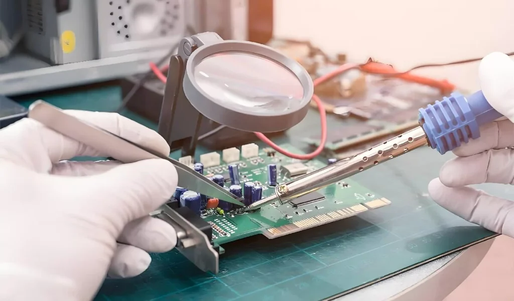
In the process of PCB horizontal plating, the following points need to be noted.
Control of plating conditions: parameters such as current density, temperature and time need to be strictly controlled to ensure the uniformity and quality of the metal layer.
Pre-treatment before plating: Before plating, the circuit board should be cleaned, degreased, descaled and other pre-treatment to ensure a good combination of plating layer and circuit board surface.
Post-plating treatment: After plating is completed, the circuit board should be cleaned, dried and other post-treatment to remove excess plating solution and residues to improve the reliability of the circuit board.
Precautions for plating line and safe production: Copper strips including auxiliary anode shall be the same length as the production board, about 5㎝ wide, and arranged close to the board; the whole board and the board after graphic plating need to be made within 24 hours for the next process. Wear fine yarn gloves for graphic plating upper boards and brown rubber gloves for lower boards, rubber gloves for full board upper boards and dry coarse yarn gloves for lower boards, and so on.
Wastewater treatment: In the process of industrial production, the use and emission of cyanide must be strictly controlled, especially there should be perfect wastewater treatment facilities to reduce the amount of cyanide discharged. Staff should wear good protection facilities such as gas masks and gloves when working to avoid the hazards of chemical substances.
Emergency treatment: In case of traveling car failure that prevents normal production, the boards should be transferred out in order, and all the boards are taken out of the insertion racks after washing in the corresponding water washing tanks and marking the cylinder number and plating time. When the stoppage time exceeds a certain length of time, it is necessary to use different flow rate of ASF to drag the cylinder to maintain the activity of the plating solution.
PCB horizontal plating technology is leading the new trend in electronics manufacturing with its excellent uniformity and high efficiency. Through continuous optimization and innovation, this technology will continue to promote the quality of electronic products and meet the high requirements of the industry.