Make PCB at home can be a rewarding experience for electronics enthusiasts and hobbyists. Whether you’re developing a new project or repairing an existing one, learning to make your own PCBs can save you money and provide valuable hands-on experience. This guide will walk you through the process of making PCBs at home, from design to fabrication, and will cover essential techniques and tips to achieve professional results.
Understanding PCB Basics
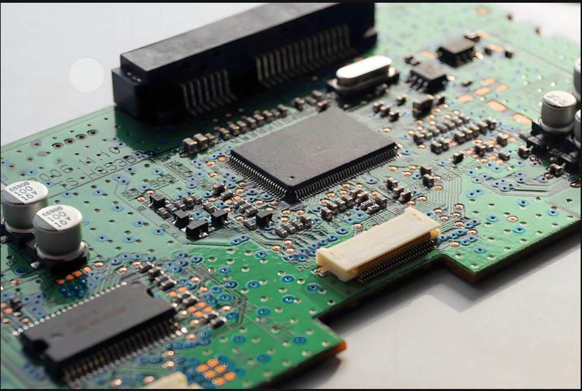
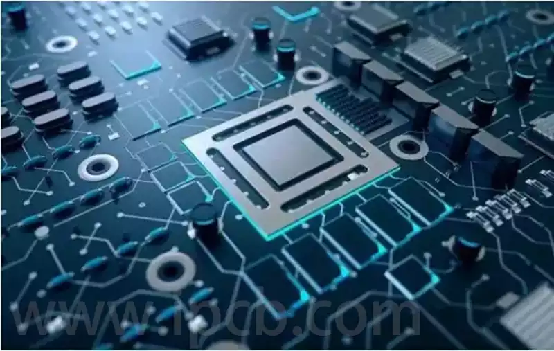
A printed circuit board (PCB) is a flat board made of insulating material, typically fiberglass or plastic, with conductive pathways etched onto its surface. These pathways, or traces, connect various electronic components to create a functioning circuit. PCBs are fundamental to almost all electronic devices, ranging from simple gadgets to complex systems.
To make a PCB at home, you’ll need to understand some basic concepts:
- PCB Design: The design phase involves creating a schematic diagram of your circuit and then converting it into a PCB layout. This layout includes the placement of components and routing of traces.
- PCB Fabrication: This is the process of creating the physical PCB from the design. It involves transferring the design onto a copper-clad board and then etching away the unwanted copper to leave behind the desired circuitry.
Materials and Tools Needed
Before you start making your PCB, gather the following materials and tools:
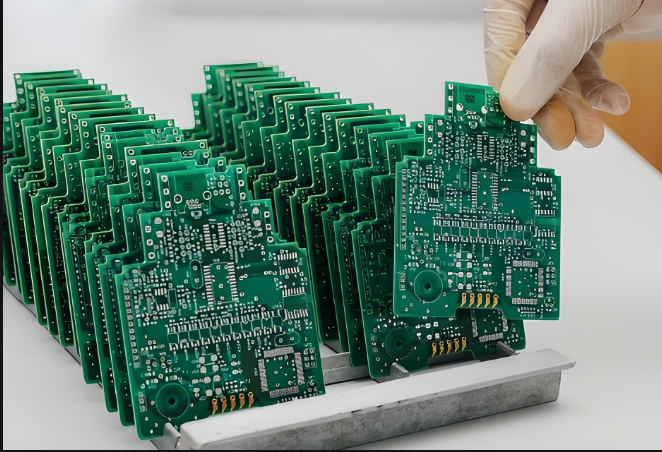
- Copper-Clad Board: This is a board coated with a thin layer of copper. It serves as the base for your PCB. Copper-clad boards come in various sizes and thicknesses. The most common type is the FR4 board, which is made of fiberglass and is suitable for most home PCB projects.
- PCB Design Software: Software such as Eagle, KiCAD, or Fritzing can be used to create and export your PCB design files. These tools offer various features, such as component libraries, schematic capture, and PCB layout design.
- Printer: A laser printer is preferred for printing your PCB design onto transfer paper. Laser printers produce a more opaque toner, which transfers better onto the copper surface. Inkjet printers are generally not recommended for this process as their ink does not adhere well to the copper.
- Transfer Paper: Special paper for transferring your PCB design onto the copper-clad board. There are different types of transfer paper available, including glossy paper and paper specifically designed for PCB fabrication.
- Etching Solution: Typically a mixture of ferric chloride or ammonium persulfate, used to remove unwanted copper. Ferric chloride is a common choice due to its effectiveness and relatively low cost. Ammonium persulfate is another option but may require more careful handling.
- Drilling Tools: A drill or a dremel tool with small bits for making holes for component leads. For precise drilling, consider using a drill press or a PCB drilling machine. Small drill bits, usually in the range of 0.3 mm to 1.0 mm, are used for most PCB hole sizes.
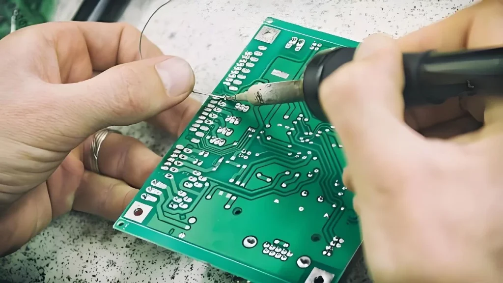
- Soldering Kit: Includes soldering iron, solder, and soldering flux for attaching components to the PCB. A temperature-controlled soldering iron is recommended for better control over the soldering process. Soldering flux helps improve the flow of solder and ensures better connections.
- Protective Gear: Safety goggles and gloves to protect yourself from chemicals and hot tools. Working with chemicals such as etching solutions can be hazardous, so proper safety measures are essential.
Step-by-Step Process
- Design Your PCBStart by designing your PCB using PCB design software. Create a schematic diagram of your circuit, then use the software to place components and route traces on the PCB layout. Ensure that your design is correct and error-free before proceeding to the next step. Export the design file in a format compatible with your PCB fabrication process, such as Gerber files.PCB design software allows you to simulate the circuit and check for errors before physical fabrication. Take advantage of these features to ensure that your design functions as intended and that there are no design rule violations.
- Print the PCB DesignPrint your PCB design onto transfer paper using a laser printer. Make sure the print is dark and clear, as this will affect the quality of the transfer. If you don’t have a laser printer, you can use a photocopier or print shop that offers high-quality prints. Ensure that the design is printed in mirror image if you are using a transfer paper method that requires this.
- Prepare the Copper-Clad BoardClean the copper-clad board with a mild abrasive or fine steel wool to remove any oxidation or dirt. Rinse the board with water and dry it thoroughly. This ensures that the copper surface is clean and ready for the design transfer. For a more thorough cleaning, you can use a specialized PCB cleaning solution or a mixture of water and baking soda.
- Transfer the DesignPlace the printed design onto the copper-clad board and use a laminator or iron to heat it. Apply even pressure and heat to transfer the toner from the paper to the copper surface. If using an iron, set it to a high temperature and press down firmly. Allow the board to cool, then carefully remove the transfer paper. Make sure that the design is fully transferred and that there are no gaps or missing sections.If you encounter issues with the toner not transferring properly, you can try increasing the temperature or extending the transfer time. Some people use a hot plate or a clothes iron to apply heat more evenly.
- Etch the PCBPrepare the etching solution according to the manufacturer’s instructions. Immerse the copper-clad board in the solution and gently agitate it to help the etching process. The solution will dissolve the unwanted copper, leaving only the traces of your design. Once the etching is complete, rinse the board with water to remove any residual chemicals.To achieve more uniform etching, ensure that the board is fully immersed and that the solution is evenly agitated. You can use a small plastic container with a lid or a dedicated etching tank for this purpose. Be patient and avoid over-etching, which can thin the traces and damage the board.
- Drill HolesUse a drill or dremel tool to make holes in the PCB for component leads. Ensure that the holes are aligned with the pads in your design. Be careful not to damage the copper traces while drilling. For precision drilling, you may need to use a drill press or a PCB-specific drilling machine.To prevent damaging the board or creating uneven holes, use a slow drilling speed and take breaks to avoid overheating. Clean the board and the drill bits regularly to remove any debris.
- Clean the PCBRemove the toner from the PCB using a solvent or abrasive pad. This step is essential to ensure a clean surface for soldering. Rinse the board with water and dry it thoroughly. You can use a specialized toner remover or a mixture of acetone and water for this purpose.
- Solder ComponentsPlace the electronic components into the holes and solder them to the PCB. Use a soldering iron and solder to secure the components in place. Apply soldering flux to improve the flow of solder and ensure strong connections. Trim any excess component leads after soldering.When soldering, ensure that each connection is well-made and that there are no solder bridges or cold joints. Inspect the board carefully to verify that all components are correctly placed and that there are no short circuits.
- Test Your PCBBefore using your PCB in a final application, test it to ensure that all connections are correct and the circuit functions as intended. Use a multimeter to check for continuity and verify that there are no short circuits. Perform a functional test to confirm that the PCB operates correctly in your application.Testing is a crucial step to ensure that the PCB performs as expected and to identify any potential issues before final assembly. Use test equipment and diagnostic tools to validate the functionality of the circuit.
Common Issues and Troubleshooting
While making PCBs at home can be a straightforward process, you may encounter some common issues. Here are a few troubleshooting tips:
- Incomplete Design Transfer: If the design does not transfer completely, check that the toner was printed dark enough and the transfer process was applied evenly. Consider using a higher-quality transfer paper or adjusting the heating time and pressure.If the toner does not adhere properly, try using a different type of transfer paper or adjusting the transfer method. Ensure that the copper surface is clean and free of oxidation before transferring the design.
- Etching Problems: Uneven etching can occur if the board is not fully immersed in the etching solution or if the solution is too weak. Ensure that the solution is fresh and that the board is evenly agitated during the process.To prevent uneven etching, use a dedicated etching tank or container and maintain proper agitation. Regularly check the solution’s concentration and replace it if necessary.
- Drilling Issues: If the drill bit breaks or the holes are misaligned, try using a slower drilling speed and ensure that the bit is sharp. Proper alignment and drilling technique can prevent these problems.Use high-quality drill bits and avoid excessive force during drilling. If possible, use a drill press for better accuracy and control.
- Soldering Difficulties: Poor solder joints can result from insufficient heating or incorrect soldering technique. Ensure that the soldering iron is properly heated and that you are applying enough solder to create solid connections.To improve soldering quality, use a temperature-controlled soldering iron and apply soldering flux to enhance the flow of solder. Practice soldering techniques on scrap boards to build proficiency.
Advantages and Limitations of Making PCBs at Home
Making PCBs at home offers several advantages:
- Cost Savings: Fabricating your own PCBs can be more cost-effective than outsourcing, especially for small quantities. You can avoid the costs associated with professional PCB manufacturing and reduce expenses for prototyping.
- Customization: You have full control over the design and fabrication process, allowing for customization to meet specific project needs. This flexibility enables you to create unique PCBs tailored to your exact specifications.
- Learning Experience: The process provides valuable hands-on experience and a deeper understanding of PCB design and fabrication. Gaining practical skills in PCB making can enhance your knowledge and improve your electronics projects.
However, there are also limitations:
- Limited Precision: Home methods may not achieve the same level of precision and quality as professional PCB manufacturing. The accuracy of home-made PCBs may be affected by factors such as design complexity and fabrication techniques.
- Time-Consuming: The process can be time-consuming and may require multiple attempts to achieve satisfactory results. Fabricating PCBs at home involves several steps, each requiring attention to detail and patience.
- Safety Concerns: Working with chemicals and hot tools requires proper safety precautions to avoid injury or exposure to harmful substances. Follow safety guidelines and use appropriate protective gear to minimize risks.
Conclusion
Making PCBs at home can be a highly rewarding endeavor for electronics enthusiasts and hobbyists. By understanding the basics of PCB design and fabrication, and following the steps outlined in this guide, you can create functional and customized PCBs for your projects. While there are challenges associated with home PCB production, the experience gained and the satisfaction of producing your own boards make it a valuable skill in the world of electronics.
If you’re new to PCB making, start with simple designs and gradually progress to more complex projects as you gain experience. With practice and patience, you’ll be able to achieve professional-quality results and enhance your skills in electronics design and fabrication. Embrace the learning process and enjoy the satisfaction of creating your own PCBs from scratch.