The number of PCB layers is the number of layers it has in the vertical direction (usually the Z-axis). In short, it is how many layers of wiring are laid on the board. Typically, PCB boards can be categorized as single-layer, double-layer, and multi-layer.
Single-layer PCB refers to the use of the same circuit wiring on both the front and back sides of the PCB board. It is cheap to produce and is suitable for simple circuit applications. However, since it can only lay one layer of circuitry on one side of the board, it has significant limitations in circuit design with dense wiring and complex interconnections.
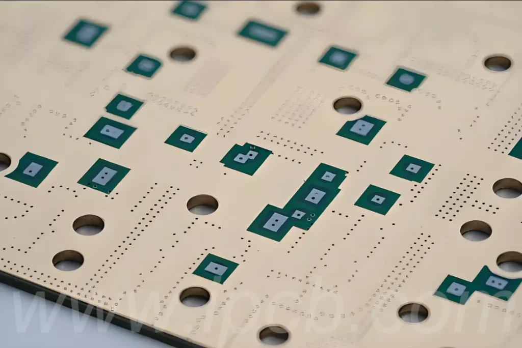
Dual-layer PCBs, on the other hand, lay one layer of wiring on each side of the board, connected by through-holes (or feed-through holes). It is suitable for moderately complex circuits, with high wiring density, narrow line width and other advantages, but the inner layer of the line is difficult to manufacture, requiring the use of complex manufacturing processes.
Multi-layer PCB is composed of three or more pcb layers of lines,and connected by through-hole. It is suitable for high-density, multi-layer, multi-signal circuits, can greatly improve the reliability and performance of the circuit board,but also requires a complex manufacturing process and high cost.
The number of PCB layers directly affects the design complexity and functionality of the board.As the number of layers increases, PCBs are better able to support more complex circuits and signaling,thus improving circuit integration and reliability.
- Signal Integrity
Increasing the number of PCB layers can significantly improve signal integrity.Multi-layer PCB design provides dedicated layers for high-speed signals,thereby reducing signal cross-talk and improving signal transmission quality.This improvement in signal integrity is particularly important for modern electronic equipment, especially in high-frequency and high-density applications. - Power and ground layer optimization
More power and ground layers can be designed to optimize power distribution, help stabilize the supply voltage in the circuit and reduce noise, which is critical for high-performance circuit boards.Setting the power and ground layers in close proximity to each other can effectively reduce the electromagnetic interference generated by the current flow guidance. - Cabling Efficiency and Design Flexibility
The multi-layer design improves wiring efficiency and makes the circuit layout more compact. Since the inner layer can be used for routing, the overall circuit can reduce the impedance and delay of signal transmission. In addition, designers have more flexibility in wiring and can flexibly adjust the function of the layer to meet different design needs. - Adapt to high-speed applications
With the increasing demand for speed and performance of electronic equipment, multi-layer PCB design came into being to meet the requirements of high-speed signal transmission.For example,card readers and high-performance computer motherboards often use multi-layer design to ensure that high-speed signals can be effectively transmitted. - Cost and Manufacturing Complexity
While multilayer PCBs offer many advantages, the manufacturing process is often more complex and costly. The manufacturing process needs to be precisely controlled to avoid problems given by multilayer designs, such as stacking deviations or through-hole problems. Therefore, when deciding on the number of layers, designers need to weigh cost against circuit performance. - Small size and light weight
Since multilayer PCBs can integrate more functionality into a smaller space, they enable the miniaturization and lightweighting of devices, adapting to the trend of modern consumer electronics. This is especially important for portable devices, which can reduce size and weight while maintaining performance. - High quality and reliability
The manufacture of multi-layer PCBs usually requires more stringent process standards,so its quality and reliability is often higher than that of single-layer and double-layer PCBs, after careful design of multi-layer PCBs can be maintained under the harsh conditions of use.
How to determine the number of PCB layers?
When you think about how to choose the number of PCB layers,you need to consider, what are the benefits of multilayer over single/double layer? Conversely, you also need to think about what are the benefits of a single layer compared to a double / multilayer? Specifically, you can consider the following 5 aspects:
- Where is the PCB used?
When considering the needs of a PCB board, you need to consider the machines and equipment that the PCB will be used in, and also determine the requirements of these machines/equipment for the circuitry of the board. Will it be used for high-tech, complex electronics or simple products with fewer features? - What operating frequency does the PCB need?
Here you need to consider the issue of operating frequency.Because the parameters of the operating frequency determine the function and capacity of the PCB. For higher speeds and operating capabilities, multilayer PCBs are essential. - What is the project budget?
Other factors to consider are the manufacturing costs of single and double layer PCBs versus multilayer PCBs.If you want PCBs with the highest possible capacity, then the cost to be paid will definitely be relatively high. - How long is the PCB delivery time required?
Delivery time, is the time required to manufacture single/double/multi-layer PCBs,when you need to manufacture PCBs in large quantities,you need to consider the delivery time. The delivery time for single/double/multi-layer PCB boards is also different,which also depends on the size of the PCB board area. Of course, if you are willing to spend more money, then the delivery time may also be shortened. - What density and signal layers are needed for the PCB?
The number of PCB layers also depends on the pin density and signal layers, e.g. a pin density of 1.0 requires 2 signal layers, and as the pin density decreases, the number of layers required increases. If the pin density is 0.2 or less, a PCB with at least 10 layers is required.
Care should be taken when designing pcb layers:
- Comprehensive consideration of layer selection
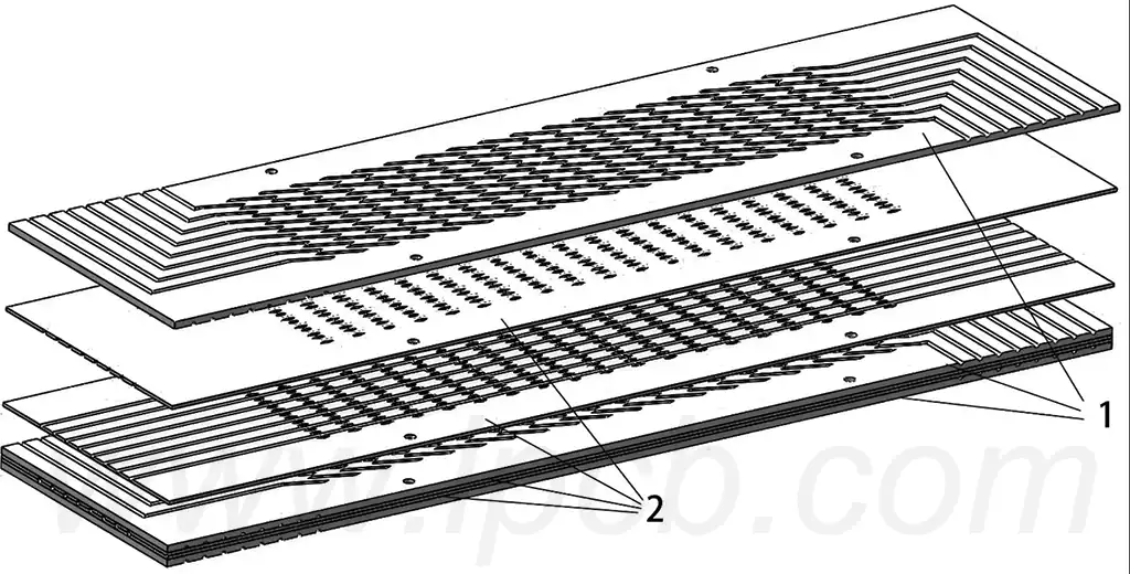
When designing the number of PCB layers, you first need to consider the wiring density of the circuit and the need for special signal lines. The choice of the number of layers not only affects the complexity of the circuit,but also directly related to the size of the board,cost and stability of manufacturing. In order to ensure signal integrity and reduce interference, it is usually recommended to use at least multi-layer boards in the design. - Separation of signal and power layers
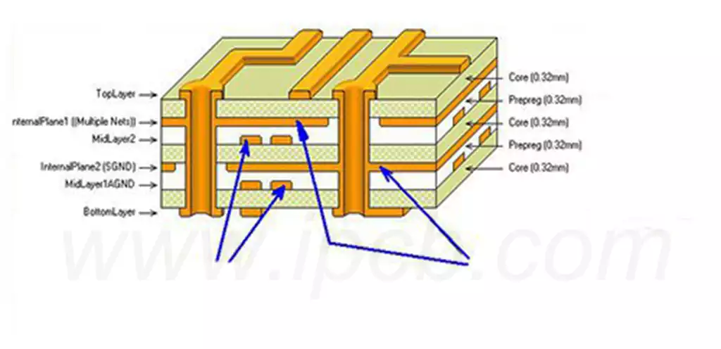
In a multilayer board design, the signal layer should be separated from the power supply layer to minimize the interference of power supply noise on the signal. This separation helps to improve signal integrity and can reduce the impact of electromagnetic interference (EMI) on circuit performance. - Cost and Manufacturing Difficulty
While increasing the number of layers can improve circuit performance, the corresponding manufacturing cost and difficulty will also increase. Circuit designers need to consider the cost-effectiveness when choosing the number of layers, balancing the performance needs and manufacturing feasibility. In general, designs with fewer layers are easier to manufacture and assemble, but this may not meet the needs of complex circuits. - Importance of Stacked Layer Construction
After selecting the number of layers, the design of the stacking structure is particularly important. Proper stacking improves the electromagnetic compatibility of the circuit and reduces crosstalk between signals. Designers need to optimize the stacking scheme according to the layout of the power and signal layers. - Materials and Characteristics
Finally, material selection should also be rationally planned according to the number of layers. Different layers of PCB using different materials will directly affect the thickness and electrical performance. Designers should use suitable insulation materials and high-quality copper foil to ensure that the PCB performance .
The choice of PCB layers is critical to the performance and reliability of the board. Factors such as usage environment, budget, operating frequency and signal requirements need to be considered during design to ensure optimal circuit performance is achieved. Proper layer selection and design will help improve the overall functionality and stability of the circuit, providing a solid foundation for modern electronic devices.