Minimum solder mask sliver (also known as solder resist) is a thin layer of polymer material applied to the surface of a PCB. Its purpose is to protect the copper circuitry and prevent solder from flowing into areas that do not need to be soldered during the soldering process. The entire circuit board is coated with soldermask, except for the pads. is the minimum allowable width of these soldermask sheets. This aspect of the design rules is critical to ensuring the reliability and manufacturability of the PCB. It is important for the following reasons:
- Manufacturability: Very thin strips of soldermask can be difficult to apply accurately during PCB manufacturing. If they are too narrow, they may not adhere properly or may be easily damaged.
- Electrical Performance: If there is a solder fillet underneath the soldermask, too thin a strip can lead to solder bridging or accidental short circuit problems.
- Mechanical Integrity: Thin strips of soldermask are more susceptible to damage during handling or assembly, which can lead to reliability issues.
What is PCB Minimum Solder mask sliver?
Minimum soldermask is a PCB process used to protect metal components on a circuit board from oxidation and to prevent conductive bridges from forming between pads. It is a critical step in PCB manufacturing, especially if reflow or solder baths are used. These techniques don’t give you much control over where bits of molten solder fall on the board, but soldermask gives you a degree of control.
Soldermask does more than just protect your PCB; it protects your PCB. it contributes to the accuracy and reliability of PCB assembly. Typically, soldermask has openings that expose copper solder pans so that components can be soldered to the PCB. A minimum gap or strip should be maintained between these openings to ensure PCB functionality and reliability. Manufacturers often set minimum electrode widths for resistive soldering to prevent problems such as solder bridging and solder absorption on core wires.
Minimum solder resist is the smallest distance between the openings of the resist layer that expose the copper pads on the PCB.
The minimum strip width depends on manufacturing tolerances and the manufacturing capabilities of the PCB. Values range from a few mils (thousands of inches) to tens of microns.
To ensure proper PCB operation, designers and manufacturers need to follow the recommended width of the soldermask, known as the minimum soldermask design rule. This rule defines the minimum width of the soldermask to avoid manufacturing problems.
You can make sure that the soldermask following the minimum soldermask rule does not interfere with the exposed copper. You should check PCB manufacturing specifications and guidelines to determine the minimum strip width for a particular project.
What is the standard solder mask sliver thickness?
The thickness of the soldermask depends primarily on the thickness of the copper traces on the board. LPSM and DPSM soldermask thicknesses in the blank areas of the board generally vary with location. Typical soldermask thickness (perpendicular to the board) is at least 0.8 mils. Near the wire edges, the soldermask thins out to 0.3 mils or less. Generally, you will need about 0.5 mils of soldermask over the traces. Sprayed epoxy soldermask provides a more uniform thickness across the PCB.
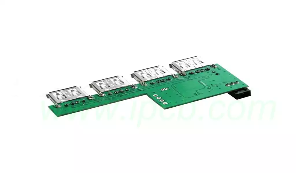
In addition to preventing corrosion of copper traces, the soldermask is used to place a barrier between adjacent pads on the board. For component pads, this is accomplished by defining a small gap between the soldermask and the exposed pad, called soldermask relief. This creates a barrier that prevents molten solder from one pad from flowing to neighboring pads. This is especially important for fine pitch BGAs and other components with high pin densities. This small relief around the pad edges allows the solder droplets to fully wet the pads and hold themselves in place, preventing bridging during the soldering process.
Impact of Minimum Solder mask Sliver Errors on PCB Designs
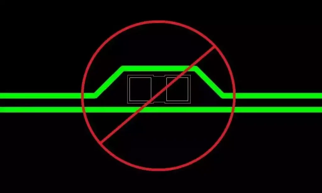
For example, there is a problem known as solder bridging. If the soldermask between two neighboring pads is too small, there is a risk that the solder will flow through the soldermask and form a solder bridge on top of the soldermask. This can lead to short circuits, wiring or component burnout, or general circuit failure.
In some cases, such as through-holes with exposed thermal pads or surface mount components, if the strip width is too small, solder may be drawn along the copper core between the openings in the soldermask. This can lead to failed solder joints and damaged electrical connections.
Additionally, manufacturing PCBs with very small soldermasks poses challenges to the manufacturing process. Higher precision and tighter tolerances are required to ensure proper application and soldermask alignment.
Prevent Problems by Using the Minimum Number of Solder Resist Layers
Reducing Minimum Soldermask Errors
Manufacturing guidelines follow minimum strip width guidelines
Prototyping and TestingPrototyping and testing prior to production
Component PlacementCheck component placement carefully
Design Rule Checking Operational DRC for your PC design
What color should the minimum solder mask sliver be?
The color of the soldermask is determined by the dye used in the soldermask material, and the chemistry of the dye affects the thickness of the cured soldermask. One reason green soldermask is widely used is that it can be used to create thin soldermask barriers (~0.1 mm). The dyes used in other colors of soldermask tend to create thicker soldermask barriers. Regardless of which dye you choose to use, the thickness of the solder resist on a PCB for a specific industry or application is defined in the IPC-SM-840D.
Soldermask color is an important part of an automated or manual visual inspection. Black soldermask provides the lowest contrast between the board and trace, which can make automated inspection difficult. This is another reason why green film is preferred. The color of the silkscreen you use can also affect visual contrast and can affect visual fatigue during manual inspection.
What solder mask sliver should I use?
Determining the proper soldermask depends on the physical size of the board, holes, components and conductors, the surface layout, and the final application of the product.
First, if your PCB soldermask will be used in the aerospace, telecom, medical, or other “high-reliability” industries, check the industry standards for soldermask and your general intended application. There are specific requirements that supersede any others you may have learned on the Internet.
For most modern printed circuit board designs, you will need a photolithographic soldermask. The surface graphics will determine whether to use a liquid or dry application. A dry application will create a uniform thickness of soldermask across the entire surface. However, if the surface of your board is very flat, a dry film will adhere best. If the surface features are complex, you’re better off with the liquid (LPSM) option for better access to the copper of the traces and the laminate. The disadvantage of liquid application is that the thickness is not completely uniform across the board.
You can also get different finishes on the laminate layers. Talk to your manufacturer about what they have available and how this will affect production. For example, if you are using a soldermask reflow process, a matte finish can reduce solder balls.

PCB Minimum Solder mask sliverTypes
All soldermasks consist of a polymer layer that is applied to the metal wires on the printed circuit board.There are many types of PCB soldermasks, and the best choice for your board depends on cost and your application. The most basic soldermask option is to use screen printing, where a liquid epoxy is printed on the conductors, much like spray painting through a stencil. Soldermask can be applied in almost any color.
- Top and Bottom Soldermask
Engineers often use these to identify openings in the green soldermask that has been applied to the PCB. This particular soldermask is added by epoxy or film methods. Next, component pins are soldered to the board using the openings that have been registered with the mask. The alignment at the top of the board is called the top alignment and the corresponding soldermask used is called the top mask. As with the top mask, the bottom mask is used on the bottom of the board. - Liquid Epoxy Soldermask
The most basic soldermask option is to use screen printing to print liquid epoxy on the PCB. This is the least expensive and most popular soldermask option. In this process, a woven mesh is used to support the ink resist pattern. Liquid epoxy is a thermosetting polymer that hardens during the heat curing process. The soldermask dye is mixed into the liquid epoxy and cures to the desired color. - Liquid Photoimageable Soldermask (LPSM)
More advanced soldermasks use a dry film or liquid resist photolithography process similar to that used for photoresist exposure in semiconductor manufacturing.LPSM can be screen printed like epoxy or sprayed onto a surface, which is often a cheaper application method. A more advanced (and accurate) method is to use a photolithography process to define soldermask openings for pads, vias, and mounting holes. - Dry Film Soldermask (DFSM)
DFSM soldermasks use a similar process to LPSM. Both PCB soldermask types are exposed during the lithography type process. Instead of a liquid coating, dry film uses a vacuum lamination process to apply the coating in the form of a soldermask foil. This vacuum lamination step forces the unexposed soldermask to adhere to the board and removes air bubbles from the film. After exposure, the unexposed areas of the soldermask are removed with a solvent, allowing the remaining film to cure in a thermal process. - Surface Preparation
Regardless of the type of PCB soldermask used, the final soldermask will leave certain exposed areas of copper on the board. These exposed areas need to be plated with a suitable surface finish to prevent oxidation. One of the most popular surface finishes is Hot Air Solder Leveling (HASL). Other surface finishes such as Electroless Nickel Palladium Immersion Gold (ENEPIC) and Electroless Nickel Immersion Gold (ENIG) can also be used upon request. When required, additional holes are left in the mask layer for pasting the mask. This paste mask is used to attach pads or other components to the board depending on the manufacturing process used.
Minimum Solder mask sliver is a thin polymer coating, usually applied to the copper surface of a printed circuit board (PCB), designed to prevent oxidation and to avoid the formation of solder bridges between closely spaced pads, i.e., an undesired electrical connection between two conductors, usually achieved with a small piece of solder. Solder mask is not necessarily used for hand-soldering components, but is critical for mass-produced boards using reflow or wave soldering techniques. Once applied, holes must be created in the soldermask by photolithography to allow connections to be made anywhere in the soldered assembly. Traditionally, the minimum solder mask sliver is green, but many other colors are available.